- 您現(xiàn)在的位置:買賣IC網(wǎng) > PDF目錄377798 > LXT305A (Digital Data Communications GmbH) Integrated T1/E1 Short-Haul Transceiver wtih Transmit JA PDF資料下載
參數(shù)資料
| 型號: | LXT305A |
| 廠商: | Digital Data Communications GmbH |
| 英文描述: | Integrated T1/E1 Short-Haul Transceiver wtih Transmit JA |
| 中文描述: | 集成的T1/E1短途收發(fā)器傳輸JA |
| 文件頁數(shù): | 6/18頁 |
| 文件大小: | 349K |
| 代理商: | LXT305A |
/;7êíè$ ,QWHJUDWHG 7ì(ì 6KRUWe+DXO 7UDQVFHLYHU ZLWK 7UDQVPLW -$
eéé
L1
7UDQVPLWWHU
Data received for transmission onto the line is clocked seri-
ally into the device at TPOS and TNEG. Input synchroni-
zation is supplied by the transmit clock (TCLK). The
transmitted pulse shape is determined by Equalizer Control
signals EC1 through EC3 as shown in Table 4. Refer to
Test Specifications for master and transmit clock timing
characteristics. Shaped pulses are applied to the AMI line
driver for transmission onto the line at TTIP and TRING.
Equalizer Control signals may be hardwired in the Hard-
ware Mode, or input as part of the serial data stream (SDI)
in the Host Mode
Pulses can be shaped for either 1.544 or 2.048 Mbps appli-
cations. 1.544 Mbps pulses for DSX-1 applications can be
programmed to match line lengths from 0 to 655 feet of
ABAM cable. The LXT305A also matches FCC and
ECSA specifications for CSU applications. 2.048 Mbps
pulses can drive coaxial or shielded twisted-pair lines.
-LWWHU $WWHQXDWLRQ
Jitter attenuation of the LXT305A transmit outputs is pro-
vided by a Jitter Attenuation Loop (JAL) and an Elastic
Store (ES). An external crystal oscillating at 4 times the bit
rate provides clock stabilization. Refer to Application
Information for crystal specifications. The ES is a 32 x 2-
bit register. Transmit data is clocked into the ES with the
transmit clock (TCLK) signal, and clocked out of the ES
with the dejittered clock from the JAL. When the bit count
in the ES is within two bits of overflowing or underflowing,
the ES adjusts the output clock by 1/8 of a bit period. The
ES produces an average delay of 16 bits in the receive path.
'ULYHU 3HUIRUPDQFH 0RQLWRU
7KH WUDQVFHLYHU LQFRUSRUDWHV D 'ULYHU 3HUIRUPDQFH 0RQLe
WRU '30 LQ SDUDOOHO ZLWK 77,3 DQG 75,1* DW WKH RXWSXW
WUDQVIRUPHU 7KH '30 RXWSXW JRHV +LJK XSRQ GHWHFWLRQ RI
ê FRQVHFXWLYH ]HURV ,W LV UHVHW ZKHQ D RQH LV GHWHFWHG RQ
WKH WUDQVPLW OLQH RU ZKHQ D UHVHW FRPPDQG LV UHFHLYHG
/LQH &RGH
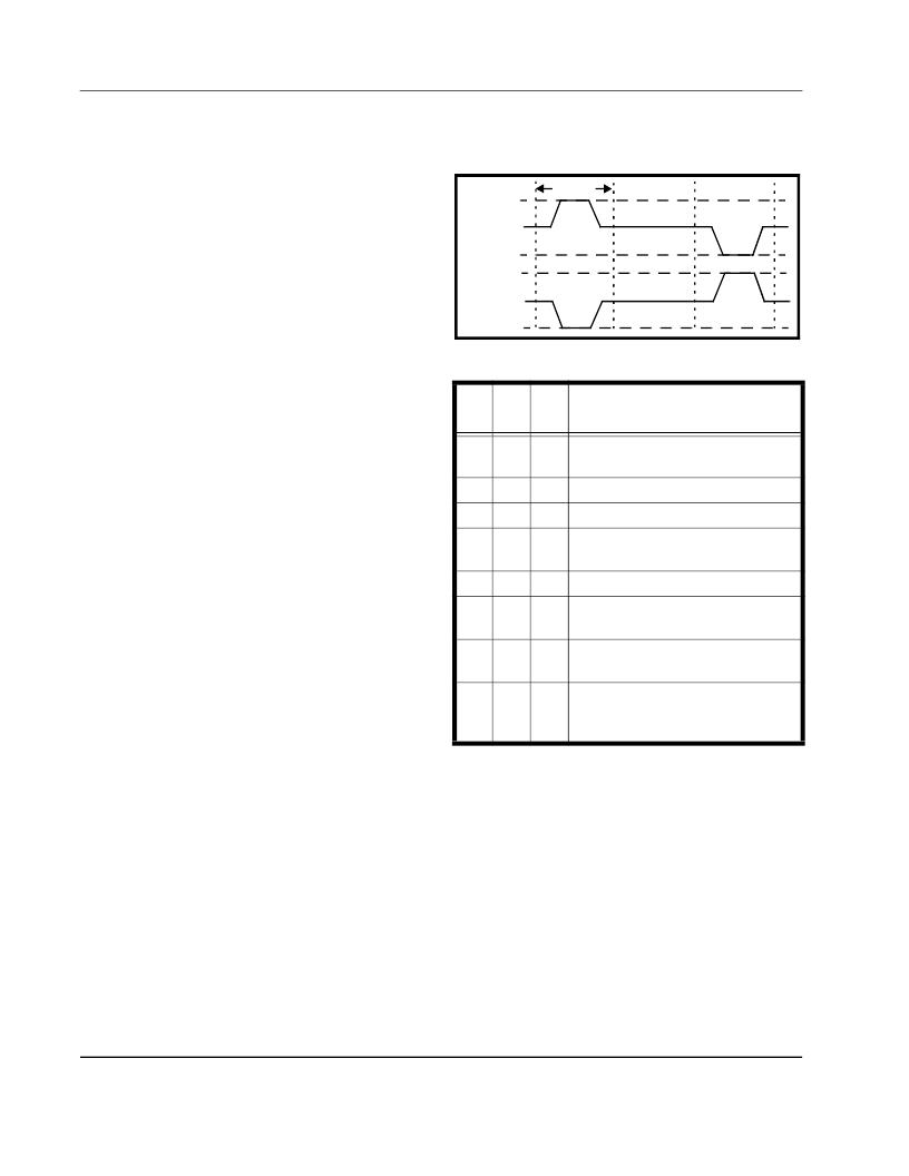
The LXT305A transmits data as a 50% AMI line code as
shown in Figure 2. The output driver maintains a constant
low output impedance regardless of whether it is driving
marks or spaces. This well controlled output impedance
provides excellent return loss (> 18 dB) when used with
external 9.1
″
precision (± 1 % accuracy) in series with a
transmit transformer with a turns ratio of 1:2.3 (± 2% accu-
racy). Series resistors also provide increased surge protec-
tion and reduced short circuit current flow.
)LJXUH èí $0, &RGLQJ
2SHUDWLQJ 0RGHV
The LXT305A can be controlled through hard-wired pins
(Hardware Mode) or by a microprocessor through a serial
interface (Host Mode). The mode of operation is set by the
MODE pin logic level. The LXT305A can also be com-
manded to operate in one of several diagnostic modes.
7DEOH /;7êíè$ 6HULDO 'DWD 2XWSXW %LWV
6HH
)LJXUH é
%LW
'è
%LW
'
%LW
'
6WDWXV
í
í
í
5HVHW KDV RFFXUUHG RU QR SURJUDP
LQSXW
í
í
ì
7$26 LV DFWLYH
í
ì
í
/RFDO /RRSEDFN LV DFWLYH
í
ì
ì
7$26 DQG /RFDO /RRSEDFN DUH
DFWLYH
ì
í
í
5HPRWH /RRSEDFN LV DFWLYH
ì
í
ì
'30 KDV FKDQJHG VWDWH VLQFH ODVW
&OHDU '30 RFFXUUHG
ì
ì
í
/26 KDV FKDQJHG VWDWH VLQFH ODVW
&OHDU /26 RFFXUUHG
ì
ì
ì
/26 DQG '30 KDYH ERWK FKDQJHG
VWDWH VLQFH ODVW &OHDU '30 DQG &OHDU
/26 RFFXUUHG
77,3
%LW &HOO
ì
ì
í
75,1*
相關(guān)PDF資料 |
PDF描述 |
|---|---|
| LXC6176 | 39513254 |
| LXC8192 | Integrated T1/E1 Short-Haul Transceiver wtih Transmit JA |
| LXT307 | PCB TERM BLK 3.5MM 7 POLE STRAGT |
| LXT310 | T1 CSU/ISDN PRI Transceiver |
| LXT312 | Low Power T1 PCM Repeaters/Transceivers |
相關(guān)代理商/技術(shù)參數(shù) |
參數(shù)描述 |
|---|---|
| LXT305AJE | 制造商:未知廠家 制造商全稱:未知廠家 功能描述:PCM Transceiver |
| LXT305ANE | 制造商:LEVEL ONE 功能描述:PCM TRANSCEIVER, Single, CEPT PCM-30/E-1, 28 Pin, Plastic, DIP 制造商:LEVELONE 功能描述:PCM TRANSCEIVER, Single, CEPT PCM-30/E-1, 28 Pin, Plastic, DIP |
| LXT305APE | 制造商:Intel 功能描述:FRAMER E1/T1 5V 28-PIN PLCC 制造商:Intel 功能描述:PCM TRANSCEIVER, Single, CEPT PCM-30/E-1, 28 Pin, Plastic, PLCC |
| LXT305JE | 制造商:未知廠家 制造商全稱:未知廠家 功能描述:PCM Transceiver |
| LXT305NE | 制造商:Level One 功能描述:PCM TRANSCEIVER, Single, CEPT PCM-30/E-1, 28 Pin, Plastic, DIP |
發(fā)布緊急采購,3分鐘左右您將得到回復。