- 您現(xiàn)在的位置:買賣IC網(wǎng) > PDF目錄358091 > M1021-13I167.2820 (INTEGRATED DEVICE TECHNOLOGY INC) ATM/SONET/SDH SUPPORT CIRCUIT, CQCC36 PDF資料下載
參數(shù)資料
| 型號(hào): | M1021-13I167.2820 |
| 廠商: | INTEGRATED DEVICE TECHNOLOGY INC |
| 元件分類: | 數(shù)字傳輸電路 |
| 英文描述: | ATM/SONET/SDH SUPPORT CIRCUIT, CQCC36 |
| 封裝: | 9 X 9 MM, CERAMIC, LCC-36 |
| 文件頁數(shù): | 4/10頁 |
| 文件大小: | 440K |
| 代理商: | M1021-13I167.2820 |
www.icst.com
●
tel (508) 852-5400
Integrated
Circuit
Systems, Inc.
M1020/21
VCSO B
ASED
C
LOCK
PLL
P r o d u c t D a t a S h e e t
General Guidelines for M and R Divider Selection
General guidelines for M/R divider selection (see
following pages for more detail):
A lower phase detector frequency should be used for
loop timing applications to assure PLL tracking,
especially during GR-253 jitter tolerance testing. The
recommended maximum phase detector frequency
for loop timing mode is
19.44MHz
. The LOL pin should
not be used during loop timing mode.
When
LOL
is to be used for system health monitoring,
the phase detector frequency should be
5MHz
or
greater. Low phase detector frequencies make
LOL
overly sensitive, and higher phase detector
frequencies make
LOL
less sensitive.
P Divider Look-Up Table (LUT)
The
P_SEL1
and
P_SEL0
pins select the post-PLL divider
values P1 and P0. The output frequency of the SAW
can be divided by
1
or
2,
or the outputs can be TriStated.
The outputs can be placed into the valid state
combinations as listed in
Table 5.
F
UNCTIONAL
D
ESCRIPTION
The M1020/21 is a PLL (Phase Locked Loop) based
clock generator that generates output clocks synchro-
nized to one of two selectable input reference clocks.
An internal high "Q" SAW delay line provides low jitter
signal performance.
A pin-selected look-up table is used to select the PLL
feedback divider (M Div) and reference divider (R Div)
as shown in Tables
3
and
4 on pg. 3
.
These look-up
tables provide flexibility in both the overall frequency
multiplication ratio (total PLL ratio) and phase detector
frequency.
The M1020/21 includes a Loss of Lock (
LOL
) indicator,
which provides status information to system
management software. A Narrow Bandwidth (
NBW
)
control pin is provided as an additional mechanism for
adjusting PLL loop bandwidth without affecting the
phase detector frequency.
Options are available for Hitless Switching (HS) with or
without Phase Build-out (PBO). They provide
SONET/SDH MTIE and TDEV compliance during a
reference clock reselection.
Input Reference Clocks
Two clock reference inputs and a selection mux are
provided. Either reference clock input can accept a
differential clock signal (such as LVPECL or LVDS) or
a single-ended clock input (LVCMOS or LVTTL on the
non-inverting input).
A single-ended reference clock on the unselected
reference input can cause an increase in output
clock jitter. For this reason, differential reference
inputs are preferred; interference from a differential
input on the non-selected input is minimal.
Implementation of single-ended input has been
facilitated by biasing
nDIF_REF0
and
nDEF_REF1
to Vcc/2,
with 50k
to Vcc and 50k
to ground. The input clock
structure, and how it is used with either
LVCMOS/LVTTL inputs or a DC- coupled LVPECL
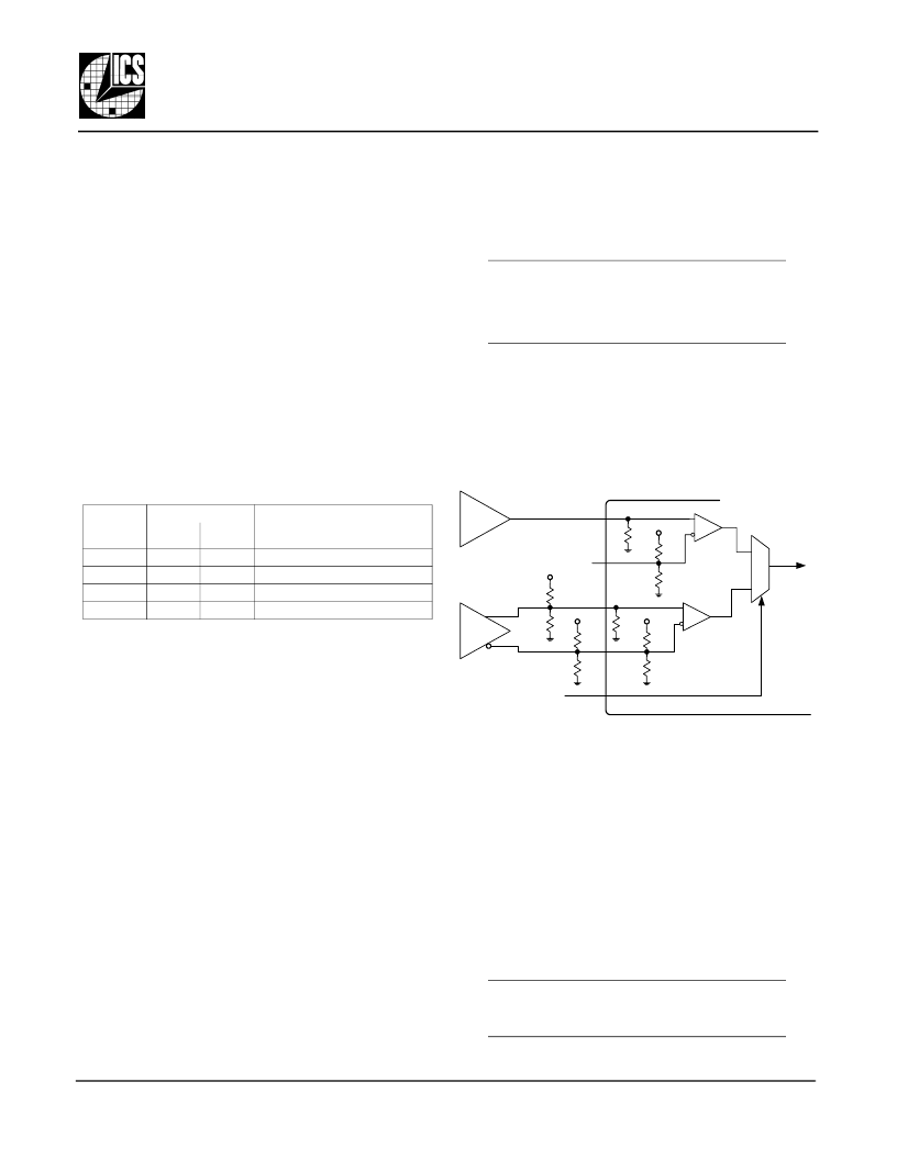
clock, is shown in Figure 4.
.
Figure 4: Input Reference Clocks
Differential LVPECL Inputs
Differential LVPECL inputs are connected to both
reference input pins in the usual manner. The external
load termination resistors shown in Figure 4 (the
127
and
82
resistors) will work for both AC and DC
coupled LVPECL reference clock lines. These provide
the
50
load termination and the VTT bias voltage.
Single-ended Inputs
Single-ended inputs (LVCMOS or LVTTL) are
connected to the non-inverting reference input pin
(
DIF_REF0
or
DIF_REF1
). The inverting reference input pin
(
nDIF_REF0
or
nDIF_REF1
) must be left unconnected.
In single-ended operation, when the unused inverting
input pin (
nDIF_REF0
or
nDEF_REF1
) is left floating (not
connected), the input will self-bias at VCC/2.
P_SEL1:0
P Values
M1020-155.5200 or M1021-155.5200
Output Frequency (MHz)
FOUT0
FOUT1
77.76 77.76
155.52 155.52
77.76 155.52
N/A N/A
Table 5: P Divider Look-Up Table (LUT)
forFOUT0 for FOUT1
0 0
0 1
1 0
1 1 TriState TriState
2
1
2
2
1
1
MUX
0
REF_SEL
1
VCC
50k
50k
VCC
50k
50k
LVCMOS/
LVPECL
50k
50k
VCC
82
127
VCC
82
127
M1020/21
X
DIF_REF0
nDIF_REF0
DIF_REF1
nDIF_REF1
相關(guān)PDF資料 |
PDF描述 |
|---|---|
| M1021-13I167.3280LF | ATM/SONET/SDH SUPPORT CIRCUIT, CQCC36 |
| M1021-13I167.3280 | ATM/SONET/SDH SUPPORT CIRCUIT, CQCC36 |
| M1021-13I167.3316LF | ATM/SONET/SDH SUPPORT CIRCUIT, CQCC36 |
| M1021-13I167.3316 | ATM/SONET/SDH SUPPORT CIRCUIT, CQCC36 |
| M1021-13I167.7097LF | ATM/SONET/SDH SUPPORT CIRCUIT, CQCC36 |
相關(guān)代理商/技術(shù)參數(shù) |
參數(shù)描述 |
|---|---|
| M10214-A1 | 功能描述:GPS模塊 GPS RF Ant Mod SiRF starIII Vertical Mnt RoHS:否 制造商:Linx Technologies 頻帶:1.575 GHz 通道數(shù)量:20 首次定位時(shí)間(冷啟動(dòng)):35 s 獲取敏感性:- 144 dBm 水平位置精確度:10 m 工作電源電壓:3 V to 4.2 V 工作電源電流:46 mA 接口類型:Serial 最大工作溫度:+ 85 C 安裝風(fēng)格:SMD/SMT 尺寸:15 mm x 13 mm x 2.2 mm |
| M10214-K1 | 功能描述:GPS開發(fā)工具 Evaluation Kit for M10214-A 2 Modules RoHS:否 制造商:STMicroelectronics 產(chǎn)品:Evaluation Boards 工具用于評(píng)估:IT600, STM32F20x 頻率:1.575 GHz 工作電源電壓:1.8 V 接口類型:Wireless |
| M10215-1F107 | 制造商: 功能描述: 制造商:undefined 功能描述: |
| M1022-3005-AL-0 | 制造商:RAF Electronic Hardware 功能描述: |
| M-102-427 | 制造商:Brady Corporation 功能描述:WIRE MARKER, SELF LAM, 0.5"W X 1.25"H, 200/ROLL; Marker Type:Self Laminating; Marker Dimensions:12.7mm x 31.75mm; Marker Material:Vinyl; Legend:Blank (No Legend); Legend Color:Black; Marker Color:White; Label Size:0.5"W x 1.25"H ;RoHS Compliant: Yes |
發(fā)布緊急采購,3分鐘左右您將得到回復(fù)。
