- 您現(xiàn)在的位置:買賣IC網(wǎng) > PDF目錄359006 > M27W512-150N6F (意法半導(dǎo)體) Quadruple D-Type Positive-Edge-Triggered Flip-Flops With Clear 16-SOIC 0 to 70 PDF資料下載
參數(shù)資料
| 型號: | M27W512-150N6F |
| 廠商: | 意法半導(dǎo)體 |
| 英文描述: | Quadruple D-Type Positive-Edge-Triggered Flip-Flops With Clear 16-SOIC 0 to 70 |
| 中文描述: | 512千位(64K的× 8)低壓紫外線EPROM和檢察官辦公室存儲器 |
| 文件頁數(shù): | 7/21頁 |
| 文件大小: | 369K |
| 代理商: | M27W512-150N6F |

7/21
M27W512
pacitors. It is recommended that a 0.1μF ceramic
capacitor be used on every device between V
CC
and V
SS
. This should be a high frequency capaci-
tor of low inherent inductance and should be
placed as close to the device as possible. In addi-
tion, a 4.7μF bulk electrolytic capacitor should be
used between V
CC
and V
SS
for every eight devic-
es. The bulk capacitor should be located near the
power supply connection point.The purpose of the
bulk capacitor is to overcome the voltage drop
caused by the inductive effects of PCB traces.
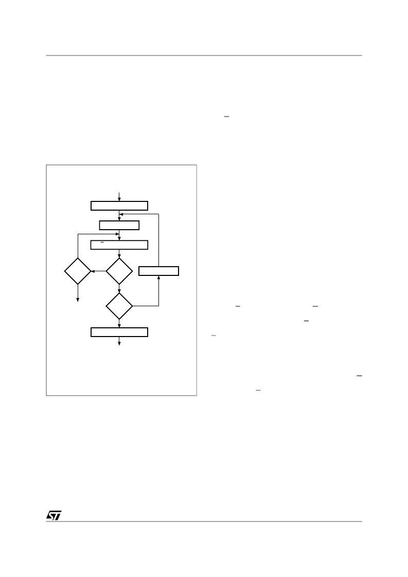
Figure 6. Programming Flowchart
Programming
The M27W512 has been designed to be fully com-
patible with the M27C512 and has the same elec-
tronic signature. As a result the M27W512 can be
programmed as the M27C512 on the same pro-
gramming equipment applying 12.75V on V
PP
and
6.25V on V
CC
. The M27W512 can use PRESTO
IIB Programming Algorithm that drastically reduc-
es the programming time. Nevertheless to achieve
compatibility with all programming equipments,
PRESTO II Programming Algorithm can be used
as well. When delivered (and after each ‘1’s era-
sure for UV EPROM), all bits of the M27W512 are
in the '1' state. Data is introduced by selectively
programming '0's into the desired bit locations. Al-
though only '0's will be programmed, both '1's and
'0's can be present in the data word. The only way
to change a ‘0’ to a ‘1’s by die exposure to ultravi-
olet light (UV EPROM). The M27W512 is in the
programming mode when V
PP
input is at 12.75V
and E is pulsed to V
IL
. The data to be programmed
is applied to 8 bits in parallel to the data output
pins. The levels required for the address and data
inputs are TTL. V
CC
is specified to be 6.25V ±
0.25V.
PRESTO IIB Programming Algorithm
PRESTO IIB Programming Algorithm allows the
whole array to be programmed with a guaranteed
margin, in a typical time of 6.5 seconds. This can
be achieved with STMicroelectronics M27W512
due to several design innovations described in the
M27W512 datasheet to improve programming ef-
ficiency and to provide adequate margin for reli-
ability. Before starting the programming the
internal MARGIN MODE circuit must be set in or-
der to guarantee that each cell is programmed with
enough margin. Then a sequence of 100μs pro-
gram pulses is applied to each byte until a correct
verify occurs (see
Figure 6.
). No overprogram
pulses are applied since the verify in MARGIN
MODE at V
CC
much higher than 3.6V, provides
the necessary margin.
Program Inhibit
Programming of multiple M27W512s in parallel
with different data is also easily accomplished. Ex-
cept for E, all like inputs including GV
PP
of the par-
allel M27W512 may be common. A TTL low level
pulse applied to a M27W512's E input, with V
PP
at
12.75V, will program that M27W512. A high level
E input inhibits the other M27W512s from being
programmed.
Program Verify
A verify (read) should be performed on the pro-
grammed bits to determine that they were correct-
ly programmed. The verify is accomplished with G
at V
IL
. Data should be verified with t
ELQV
after the
falling edge of E.
Electronic Signature
The Electronic Signature (ES) mode allows the
reading out of a binary code from an EPROM that
will identify its manufacturer and type. This mode
is intended for use by programming equipment to
automatically match the device to be programmed
with its corresponding programming algorithm.
The ES mode is functional in the 25°C ± 5°C am-
bient temperature range that is required when pro-
gramming the M27W512. To activate the ES
mode, the programming equipment must force
11.5V to 12.5V on address line A9 of the
M27W512. Two identifier bytes may then be se-
AI00738C
n = 0
Last
Addr
VERIFY
E = 100
μ
s Pulse
++n
= 25
++ Addr
VCC = 6.25V, VPP = 12.75V
FAIL
CHECK ALL BYTES
1st: VCC = 5V
2nd: VCC = 2.7V
YES
NO
YES
NO
YES
NO
SET MARGIN MODE
RESET MARGIN MODE
相關(guān)PDF資料 |
PDF描述 |
|---|---|
| M27W512-150N6TR | Quadruple D-Type Positive-Edge-Triggered Flip-Flops With Clear 16-SOIC 0 to 70 |
| M27W512-200B6 | Quadruple D-Type Positive-Edge-Triggered Flip-Flops With Clear 16-SOIC 0 to 70 |
| M27W512-200B6E | Quadruple D-Type Positive-Edge-Triggered Flip-Flops With Clear 16-SOIC 0 to 70 |
| M27W512-200B6F | Quadruple D-Type Positive-Edge-Triggered Flip-Flops With Clear 16-PDIP 0 to 70 |
| M27W512-200B6TR | Quadruple D-Type Positive-Edge-Triggered Flip-Flops With Clear 16-PDIP 0 to 70 |
相關(guān)代理商/技術(shù)參數(shù) |
參數(shù)描述 |
|---|---|
| M27W512-150N6TR | 制造商:STMICROELECTRONICS 制造商全稱:STMicroelectronics 功能描述:512 Kbit 64Kb x8 Low Voltage UV EPROM and OTP EPROM |
| M27W512-200B6 | 制造商:STMICROELECTRONICS 制造商全稱:STMicroelectronics 功能描述:512 Kbit (64K x8) Low Voltage UV EPROM and OTP EPROM |
| M27W512-200B6E | 制造商:STMICROELECTRONICS 制造商全稱:STMicroelectronics 功能描述:512 Kbit (64K x8) Low Voltage UV EPROM and OTP EPROM |
| M27W512-200B6F | 制造商:STMICROELECTRONICS 制造商全稱:STMicroelectronics 功能描述:512 Kbit (64K x8) Low Voltage UV EPROM and OTP EPROM |
| M27W512-200B6TR | 制造商:STMICROELECTRONICS 制造商全稱:STMicroelectronics 功能描述:512 Kbit 64Kb x8 Low Voltage UV EPROM and OTP EPROM |
發(fā)布緊急采購,3分鐘左右您將得到回復(fù)。