- 您現(xiàn)在的位置:買賣IC網(wǎng) > PDF目錄359025 > M29F040-90XK1R (意法半導(dǎo)體) 4 Mbit 512Kb x8, Uniform Block Single Supply Flash Memory PDF資料下載
參數(shù)資料
| 型號: | M29F040-90XK1R |
| 廠商: | 意法半導(dǎo)體 |
| 英文描述: | 4 Mbit 512Kb x8, Uniform Block Single Supply Flash Memory |
| 中文描述: | 4兆位512KB的× 8,統(tǒng)一座單電源閃存 |
| 文件頁數(shù): | 7/31頁 |
| 文件大?。?/td> | 232K |
| 代理商: | M29F040-90XK1R |
第1頁第2頁第3頁第4頁第5頁第6頁當(dāng)前第7頁第8頁第9頁第10頁第11頁第12頁第13頁第14頁第15頁第16頁第17頁第18頁第19頁第20頁第21頁第22頁第23頁第24頁第25頁第26頁第27頁第28頁第29頁第30頁第31頁

64K Bytes Block
AI01362B
7FFFFh
6FFFFh
5FFFFh
4FFFFh
3FFFFh
2FFFFh
1FFFFh
0FFFFh
TOP
ADDRESS
70000h
60000h
50000h
40000h
30000h
20000h
10000h
00000h
BOTTOM
ADDRESS
A18
1
1
64K Bytes Block
64K Bytes Block
64K Bytes Block
64K Bytes Block
A17
1
1
A16
1
0
1
1
0
0
1
0
0
0
1
1
1
0
0
0
1
0
0
0
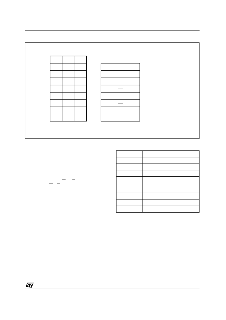
Figure 3. Memory Map and Block Address Table
Hex Code
Command
00h
Read
10h
Chip Erase Confirm
30h
Block Erase Resume/Confirm
80h
Set-up Erase
90h
Read Electronic Signature/
Block Protection Status
A0h
Program
B0h
Erase Suspend
F0h
Read Array/Reset
Table 7. Commands
Instructions and Commands
The Command Interface (C.I.) latches commands
written to the memory. Instructions are made up
from one or more commands to perform Read
Array/Reset, Read Electronic Signature, Block
Erase, Chip Erase, Program, Block Erase Suspend
and Erase Resume. Commands are made of ad-
dress and data sequences. Addresses are latched
on the falling edge of W or E and data is latched
on the rising of W or E. The instructions require from
1 to 6 cycles, the first or first three of which are
always write operations used to initiate the com-
mand. They are followed by either further write
cycles to confirm the first command or execute the
command immediately. Command sequencing
must be followed exactly. Any invalid combination
of commands will reset the device to Read Array.
The increased number of cycles has been chosen
to assure maximum data security. Commands are
initialised by two preceding coded cycles which
unlock the Command Interface. In addition, for
Erase, command confirmation is again preceeded
by the two coded cycles.
P/E.C. status is indicated during command execu-
tion by Data Polling on DQ7, detection of Toggle on
DQ6, or Error on DQ5 and Erase Timer DQ3 bits.
Any read attempt during Program or Erase com-
mand execution will automatically output those four
bits. The P/E.C. automatically sets bits DQ3, DQ5,
DQ6 and DQ7. Other bits (DQ0, DQ1, DQ2 and
DQ4) are reserved for future use and should be
masked.
7/31
M29F040
相關(guān)PDF資料 |
PDF描述 |
|---|---|
| M29F040-120XK1R | 4 Mbit 512Kb x8, Uniform Block Single Supply Flash Memory |
| M29F040-150XK1R | 4 Mbit 512Kb x8, Uniform Block Single Supply Flash Memory |
| M29F040-70XK6R | 4 Mbit 512Kb x8, Uniform Block Single Supply Flash Memory |
| M29F040-90XK6R | 4 Mbit 512Kb x8, Uniform Block Single Supply Flash Memory |
| M29F040-120XK6R | 4 Mbit 512Kb x8, Uniform Block Single Supply Flash Memory |
相關(guān)代理商/技術(shù)參數(shù) |
參數(shù)描述 |
|---|---|
| M29F040-90XK1TR | 制造商:STMICROELECTRONICS 制造商全稱:STMicroelectronics 功能描述:4 Mbit 512Kb x8, Uniform Block Single Supply Flash Memory |
| M29F040-90XK3R | 制造商:STMICROELECTRONICS 制造商全稱:STMicroelectronics 功能描述:4 Mbit 512Kb x8, Uniform Block Single Supply Flash Memory |
| M29F040-90XK3TR | 制造商:STMICROELECTRONICS 制造商全稱:STMicroelectronics 功能描述:4 Mbit 512Kb x8, Uniform Block Single Supply Flash Memory |
| M29F040-90XK5R | 制造商:STMICROELECTRONICS 制造商全稱:STMicroelectronics 功能描述:4 Mbit 512Kb x8, Uniform Block Single Supply Flash Memory |
| M29F040-90XK5TR | 制造商:STMICROELECTRONICS 制造商全稱:STMicroelectronics 功能描述:4 Mbit 512Kb x8, Uniform Block Single Supply Flash Memory |
發(fā)布緊急采購,3分鐘左右您將得到回復(fù)。