- 您現在的位置:買賣IC網 > PDF目錄370830 > M30218 (Mitsubishi Electric Corporation) SINGLE-CHIP 16-BIT CMOS MICROCOMPUTER PDF資料下載
參數資料
| 型號: | M30218 |
| 廠商: | Mitsubishi Electric Corporation |
| 英文描述: | SINGLE-CHIP 16-BIT CMOS MICROCOMPUTER |
| 中文描述: | 單片16位CMOS微機 |
| 文件頁數: | 108/467頁 |
| 文件大小: | 4984K |
| 代理商: | M30218 |
第1頁第2頁第3頁第4頁第5頁第6頁第7頁第8頁第9頁第10頁第11頁第12頁第13頁第14頁第15頁第16頁第17頁第18頁第19頁第20頁第21頁第22頁第23頁第24頁第25頁第26頁第27頁第28頁第29頁第30頁第31頁第32頁第33頁第34頁第35頁第36頁第37頁第38頁第39頁第40頁第41頁第42頁第43頁第44頁第45頁第46頁第47頁第48頁第49頁第50頁第51頁第52頁第53頁第54頁第55頁第56頁第57頁第58頁第59頁第60頁第61頁第62頁第63頁第64頁第65頁第66頁第67頁第68頁第69頁第70頁第71頁第72頁第73頁第74頁第75頁第76頁第77頁第78頁第79頁第80頁第81頁第82頁第83頁第84頁第85頁第86頁第87頁第88頁第89頁第90頁第91頁第92頁第93頁第94頁第95頁第96頁第97頁第98頁第99頁第100頁第101頁第102頁第103頁第104頁第105頁第106頁第107頁當前第108頁第109頁第110頁第111頁第112頁第113頁第114頁第115頁第116頁第117頁第118頁第119頁第120頁第121頁第122頁第123頁第124頁第125頁第126頁第127頁第128頁第129頁第130頁第131頁第132頁第133頁第134頁第135頁第136頁第137頁第138頁第139頁第140頁第141頁第142頁第143頁第144頁第145頁第146頁第147頁第148頁第149頁第150頁第151頁第152頁第153頁第154頁第155頁第156頁第157頁第158頁第159頁第160頁第161頁第162頁第163頁第164頁第165頁第166頁第167頁第168頁第169頁第170頁第171頁第172頁第173頁第174頁第175頁第176頁第177頁第178頁第179頁第180頁第181頁第182頁第183頁第184頁第185頁第186頁第187頁第188頁第189頁第190頁第191頁第192頁第193頁第194頁第195頁第196頁第197頁第198頁第199頁第200頁第201頁第202頁第203頁第204頁第205頁第206頁第207頁第208頁第209頁第210頁第211頁第212頁第213頁第214頁第215頁第216頁第217頁第218頁第219頁第220頁第221頁第222頁第223頁第224頁第225頁第226頁第227頁第228頁第229頁第230頁第231頁第232頁第233頁第234頁第235頁第236頁第237頁第238頁第239頁第240頁第241頁第242頁第243頁第244頁第245頁第246頁第247頁第248頁第249頁第250頁第251頁第252頁第253頁第254頁第255頁第256頁第257頁第258頁第259頁第260頁第261頁第262頁第263頁第264頁第265頁第266頁第267頁第268頁第269頁第270頁第271頁第272頁第273頁第274頁第275頁第276頁第277頁第278頁第279頁第280頁第281頁第282頁第283頁第284頁第285頁第286頁第287頁第288頁第289頁第290頁第291頁第292頁第293頁第294頁第295頁第296頁第297頁第298頁第299頁第300頁第301頁第302頁第303頁第304頁第305頁第306頁第307頁第308頁第309頁第310頁第311頁第312頁第313頁第314頁第315頁第316頁第317頁第318頁第319頁第320頁第321頁第322頁第323頁第324頁第325頁第326頁第327頁第328頁第329頁第330頁第331頁第332頁第333頁第334頁第335頁第336頁第337頁第338頁第339頁第340頁第341頁第342頁第343頁第344頁第345頁第346頁第347頁第348頁第349頁第350頁第351頁第352頁第353頁第354頁第355頁第356頁第357頁第358頁第359頁第360頁第361頁第362頁第363頁第364頁第365頁第366頁第367頁第368頁第369頁第370頁第371頁第372頁第373頁第374頁第375頁第376頁第377頁第378頁第379頁第380頁第381頁第382頁第383頁第384頁第385頁第386頁第387頁第388頁第389頁第390頁第391頁第392頁第393頁第394頁第395頁第396頁第397頁第398頁第399頁第400頁第401頁第402頁第403頁第404頁第405頁第406頁第407頁第408頁第409頁第410頁第411頁第412頁第413頁第414頁第415頁第416頁第417頁第418頁第419頁第420頁第421頁第422頁第423頁第424頁第425頁第426頁第427頁第428頁第429頁第430頁第431頁第432頁第433頁第434頁第435頁第436頁第437頁第438頁第439頁第440頁第441頁第442頁第443頁第444頁第445頁第446頁第447頁第448頁第449頁第450頁第451頁第452頁第453頁第454頁第455頁第456頁第457頁第458頁第459頁第460頁第461頁第462頁第463頁第464頁第465頁第466頁第467頁
94
Serial I/O
M
i
t
s
u
M
S
b
i
s
3
M
h
0
I
C
i
m
2
R
i
1
O
c
r
8
C
o
c
o
G
M
m
p
r
P
u
t
u
T
e
r
p
R
s
o
U
S
I
N
G
L
E
-
C
H
I
P
1
6
-
B
I
T
C
M
O
O
E
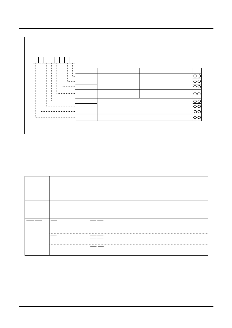
Figure 79. UARTi transmit/receive mode register in clock synchronous serial I/O mode (i=0,1)
Table 25 lists the functions of the input/output pins during clock synchronous serial I/O mode. Note that
for a period from when the UARTi operation mode is selected to when transfer starts, the TxDi pin outputs
a “H”. (If the N-channel open-drain is selected, this pin is in floating state.)
Table 25. Input/output pin functions in clock synchronous serial I/O mode (i=0,1)
Symbol
UiMR(i=0,1)
Address
03A0
16
, 03A8
16
When reset
00
16
CKDIR
UARTi transmit/receive mode register
Internal/external clock
select bit
STPS
PRY
PRYE
SLEP
0 : Internal clock
1 : External clock
Bit name
Function
Bit symbol
W
R
b7
0
b6
b5
b4
b3
b2
0
b1
0 1
b0
0 (Must always be "0" in clock synchronous serial I/O mode)
SMD0
SMD1
SMD2
Serial I/O mode select bit
0 0 1 : Clock synchronous serial
I/O mode
b2 b1 b0
Invalid in clock synchronous serial I/O mode
Pin name
Function
Method of selection
TxDi
(P4
4
, P7
4
)
RxDi
(P4
5
, P7
5
)
Serial data output
Serial data input
Transfer clock output
Transfer clock input
Programmable I/O port
(Outputs dummy data when performing reception only)
CLKi
(P4
6
, P7
6
)
Internal/external clock select bit (bit 3 at address 03A0
16
, 03A8
16
) = “0”
Internal/external clock select bit (bit 3 at address 03A0
16
, 03A8
16
) = “1”
Port P4
6
, P7
6
direction register (bits 6 at address 03EA
16
and 03EF
16
) = “0”
Port P4
5
, P7
5
direction register (bits 5 at address 03EA
16
and 03EF
16
)= “0”
(Can be used as an input port when performing transmission only)
CTS/RTS disable bit (bit 4 at address 03A4
16
, 03AC
16
) =“0”
CTS/RTS function select bit (bit 2 at address 03A4
16
, 03AC
16
) = “0”
Port P4
7
, P7
7
direction register (bits 7 address 03EA
16
and 03EF16
) = “0”
CTS/RTS disable bit (bit 4 at address 03A4
16
, 03AC
16
)
= “0”
CTS/RTS function select bit (bit 2 at address 03A4
16
, 03AC
16
) = “1”
CTS/RTS disable bit (bit 4 at address 03A4
16
, 03AC
16
) = “1”
CTS input
RTS output
CTSi/RTSi
(P4
7
, P7
7
)
相關PDF資料 |
PDF描述 |
|---|---|
| M30218FA | SINGLE-CHIP 16-BIT CMOS MICROCOMPUTER |
| M30218FC | SINGLE-CHIP 16-BIT CMOS MICROCOMPUTER |
| M30218FCFP | SINGLE-CHIP 16-BIT CMOS MICROCOMPUTER |
| M30218MC | SINGLE-CHIP 16-BIT CMOS MICROCOMPUTER |
| M30220MA-101GP | RES-ARRAY 100-OHM 2-ELEMENT 5% 0.063W CONVEX THK-FILM SMD-0505 TR-7-PA |
相關代理商/技術參數 |
參數描述 |
|---|---|
| M30218FA | 制造商:MITSUBISHI 制造商全稱:Mitsubishi Electric Semiconductor 功能描述:SINGLE-CHIP 16-BIT CMOS MICROCOMPUTER |
| M30218FC | 制造商:MITSUBISHI 制造商全稱:Mitsubishi Electric Semiconductor 功能描述:SINGLE-CHIP 16-BIT CMOS MICROCOMPUTER |
| M30218FCFP | 制造商:MITSUBISHI 制造商全稱:Mitsubishi Electric Semiconductor 功能描述:SINGLE-CHIP 16-BIT CMOS MICROCOMPUTER |
| M30218MA | 制造商:MITSUBISHI 制造商全稱:Mitsubishi Electric Semiconductor 功能描述:SINGLE-CHIP 16-BIT CMOS MICROCOMPUTER |
| M30218MAA101 | 制造商:Panasonic Industrial Company 功能描述:IC |
發(fā)布緊急采購,3分鐘左右您將得到回復。