- 您現(xiàn)在的位置:買賣IC網(wǎng) > PDF目錄370830 > M30220FA (Mitsubishi Electric Corporation) SINGLE-CHIP 16-BIT CMOS MICROCOMPUTER PDF資料下載
參數(shù)資料
| 型號(hào): | M30220FA |
| 廠商: | Mitsubishi Electric Corporation |
| 英文描述: | SINGLE-CHIP 16-BIT CMOS MICROCOMPUTER |
| 中文描述: | 單片16位CMOS微機(jī) |
| 文件頁數(shù): | 173/212頁 |
| 文件大小: | 2891K |
| 代理商: | M30220FA |
第1頁第2頁第3頁第4頁第5頁第6頁第7頁第8頁第9頁第10頁第11頁第12頁第13頁第14頁第15頁第16頁第17頁第18頁第19頁第20頁第21頁第22頁第23頁第24頁第25頁第26頁第27頁第28頁第29頁第30頁第31頁第32頁第33頁第34頁第35頁第36頁第37頁第38頁第39頁第40頁第41頁第42頁第43頁第44頁第45頁第46頁第47頁第48頁第49頁第50頁第51頁第52頁第53頁第54頁第55頁第56頁第57頁第58頁第59頁第60頁第61頁第62頁第63頁第64頁第65頁第66頁第67頁第68頁第69頁第70頁第71頁第72頁第73頁第74頁第75頁第76頁第77頁第78頁第79頁第80頁第81頁第82頁第83頁第84頁第85頁第86頁第87頁第88頁第89頁第90頁第91頁第92頁第93頁第94頁第95頁第96頁第97頁第98頁第99頁第100頁第101頁第102頁第103頁第104頁第105頁第106頁第107頁第108頁第109頁第110頁第111頁第112頁第113頁第114頁第115頁第116頁第117頁第118頁第119頁第120頁第121頁第122頁第123頁第124頁第125頁第126頁第127頁第128頁第129頁第130頁第131頁第132頁第133頁第134頁第135頁第136頁第137頁第138頁第139頁第140頁第141頁第142頁第143頁第144頁第145頁第146頁第147頁第148頁第149頁第150頁第151頁第152頁第153頁第154頁第155頁第156頁第157頁第158頁第159頁第160頁第161頁第162頁第163頁第164頁第165頁第166頁第167頁第168頁第169頁第170頁第171頁第172頁當(dāng)前第173頁第174頁第175頁第176頁第177頁第178頁第179頁第180頁第181頁第182頁第183頁第184頁第185頁第186頁第187頁第188頁第189頁第190頁第191頁第192頁第193頁第194頁第195頁第196頁第197頁第198頁第199頁第200頁第201頁第202頁第203頁第204頁第205頁第206頁第207頁第208頁第209頁第210頁第211頁第212頁
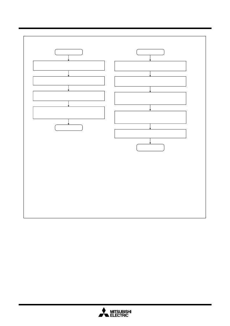
CPU Rewrite Mode (Flash Memory Version)
deeopmen
Preliminary Specifications REV.E
Specifications in this manual are tentative and subject to change.
Mitsubishi microcomputers
M30220 Group
SINGLE-CHIP 16-BIT CMOS MICROCOMPUTER
173
End
Start
Execute read array command or reset flash
memory by setting flash memory reset bit (by
writing “1” and then “0” in succession) (Note 4)
Single-chip mode, or boot mode (Note 1)
Set processor mode register (Note 2)
Using software command execute erase,
program, or other operation
Jump to transferred control program in RAM
(Subsequent operations are executed by control
program in this RAM)
Transfer CPU rewrite mode control
program to internal RAM
Note 1: Apply 5V ± 10 % to CNV
SS
pin by confirmation of CPU rewrite mode entry flag when started operation
with single-chip mode.
Note 2: During CPU rewrite mode, set the main clock frequency as shown below using the main clock divide ratio
select bit (bit 6 at address 0006
16
and bits 6 and 7 at address 0007
16
):
5.0 MHz or less when wait bit (bit 7 at address 0005
16
) = “0” (without internal access wait state)
10.0 MHz or less when wait bit (bit 7 at address 0005
16
) = “1” (with internal access wait state)
Note 3: For CPU rewrite mode select bit to be set to “1”, the user needs to write a “0” and then a “1” to it in
succession. When it is not this procedure, it is not enacted in “1”. This is necessary to ensure that no
interrupt or DMA transfer will be executed during the interval.
Note 4: Before exiting the CPU rewrite mode after completing erase or program operation, always be sure to
execute a read array command or reset the flash memory.
Write “0” to CPU rewrite mode select bit
Set CPU rewrite mode select bit to “1” (by
writing “0” and then “1” in succession)(Note 3)
Check the CPU rewrite mode entry flag
*1
*1
Program in ROM
Program in RAM
Figure 1.23.2. CPU rewrite mode set/reset flowchart
相關(guān)PDF資料 |
PDF描述 |
|---|---|
| M30220FC | SINGLE-CHIP 16-BIT CMOS MICROCOMPUTER |
| M30220FCGP | SINGLE-CHIP 16-BIT CMOS MICROCOMPUTER |
| M30220FCRP | SINGLE-CHIP 16-BIT CMOS MICROCOMPUTER |
| M30220MA | SINGLE-CHIP 16-BIT CMOS MICROCOMPUTER |
| M30220MC | SINGLE-CHIP 16-BIT CMOS MICROCOMPUTER |
相關(guān)代理商/技術(shù)參數(shù) |
參數(shù)描述 |
|---|---|
| M30220FA-XXXGP | 制造商:RENESAS 制造商全稱:Renesas Technology Corp 功能描述:SINGLE-CHIP 16-BIT CMOS MICROCOMPUTER |
| M30220FA-XXXRP | 制造商:RENESAS 制造商全稱:Renesas Technology Corp 功能描述:SINGLE-CHIP 16-BIT CMOS MICROCOMPUTER |
| M30220FC | 制造商:MITSUBISHI 制造商全稱:Mitsubishi Electric Semiconductor 功能描述:SINGLE-CHIP 16-BIT CMOS MICROCOMPUTER |
| M30220FCGP | 制造商:Renesas Electronics Corporation 功能描述:M16C 128K/10K, 10MHZ,A-D,D-A,WDT/LCD DR - Trays |
| M30220FCGP#D3 | 制造商:Renesas Electronics Corporation 功能描述: |
發(fā)布緊急采購,3分鐘左右您將得到回復(fù)。