- 您現(xiàn)在的位置:買賣IC網(wǎng) > PDF目錄377824 > M34S32MN1T (意法半導體) 32K Serial I2C Bus EEPROM With User-Defined Read-Only Block and 32-Byte OTP Page PDF資料下載
參數(shù)資料
| 型號: | M34S32MN1T |
| 廠商: | 意法半導體 |
| 元件分類: | DRAM |
| 英文描述: | 32K Serial I2C Bus EEPROM With User-Defined Read-Only Block and 32-Byte OTP Page |
| 中文描述: | 32K的串行I2C總線的EEPROM與用戶定義的只讀塊和32字節(jié)檢察官頁 |
| 文件頁數(shù): | 9/18頁 |
| 文件大小: | 156K |
| 代理商: | M34S32MN1T |
M34S32
9/18
Write to the Control Register
The control register is accessed using a specific
Device Select Byte (as described in Table 3, and
as shown in Table 11 and Table 12).
The meanings of the bits in Table 11 can be sum-
marised as follows:
WCpol.
This bit controls the polarity of the WC in-
put (to switch pin 7 between being a WC or WC in-
put). The default (initial) state of this bit is 0.
CRWD.
This is the Control Register Write Disable
bit. When it is 0, pin 3 is a Don’t Care input, and the
control register is always writable. This is the de-
fault (initial) condition of this bit.
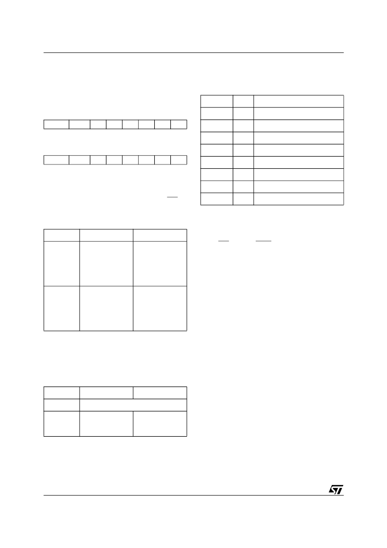
Table 11. Content of the Control Register
b7
b6
b5
CRWD WCpol
X
b4
B2
b3
B1
b2
B0
b1
X
b0
X
Table 12. Default values
b7
b6
0
0
b5
X
b4
0
b3
0
b2
0
b1
X
b0
X
Table 13. Operation of the WCpol Bit
pin 7 = high
pin 7 = low
WCpol = 0
Whole EEPROM
and OTP page are
write protected
Write instructions
are allowed in the
EEPROM area,
and the OTP
page can be
written once
WCpol = 1
Write instructions
are allowed in the
EEPROM area,
and the OTP
page can be
written once
Whole EEPROM
and OTP page are
write protected
Table 14. Operation of the CRWD Bit
pin 3 = high
pin 3 = low
CRWD = 0
Control register is writable
CRWD = 1
Control register is
writable
Control register is
write protected
(read only)
B2,B1,B0.
These bits control the size of the ROM
block. Their initial, default state is 0, 0, 0.
In all cases, except when (B2,B1,B0)=(0,0,0), the
selected area of EEPROM becomes read only
(Write Protected) regardless of the status of the
other bits and pins. However, the Control Register
itself remains alterable in accordance with the sta-
tus of WC, WCpol, WCR and CRWD.
Write to the OTP Page
The OTP page is accessed by addressing the de-
vice using the specific, Device Select Byte (as de-
scribed in Table 3).
The correct sequence for this instruction can be
sketched out as follows:
Start
OTP Page Select(= 1010 0010)
Ack
Address (MSB) (= xxxx 0000)
Ack
Address (LSB) (= 0000 0000)
Ack
Data
(= byte to be written)
Ack
........
Data
(= byte to be written)
Ack
Stop
If one bit of the OTP Page Select differs from the
above values, the OTP Page Select will NOT be
acknowledged and the WRITE instruction will be
ignored.
Table 15. Operation of the B2, B1 and B0 Bits
B2,B1,B0
ROM block size and location
0,0,0
0
All bits are EEPROM
0,0,1
1/64
ROM block=00h to 01FFh (512)
0,1,0
1/32
ROM block=00h to 03FFh (1K)
0,1,1
1/16
ROM block=00h to 07FFh (2K)
1,0,0
1/8
ROM block=00h to 0FFFh (4K)
1,0,1
1/4
ROM block=00h to 1FFFh (8K)
1,1,0
1/2
ROM block=00h to 3FFFh (16K)
1,1,1
1
All bits are ROM
相關PDF資料 |
PDF描述 |
|---|---|
| M34S32MN5T | 32K Serial I2C Bus EEPROM With User-Defined Read-Only Block and 32-Byte OTP Page |
| M34S32MN6T | 32K Serial I2C Bus EEPROM With User-Defined Read-Only Block and 32-Byte OTP Page |
| M34S32WBN6T | 32K Serial I2C Bus EEPROM With User-Defined Read-Only Block and 32-Byte OTP Page |
| M34S32WMN5T | 32K Serial I2C Bus EEPROM With User-Defined Read-Only Block and 32-Byte OTP Page |
| M34S32WMN6T | 32K Serial I2C Bus EEPROM With User-Defined Read-Only Block and 32-Byte OTP Page |
相關代理商/技術參數(shù) |
參數(shù)描述 |
|---|---|
| M34S32MN5T | 制造商:STMICROELECTRONICS 制造商全稱:STMicroelectronics 功能描述:32K Serial I2C Bus EEPROM With User-Defined Read-Only Block and 32-Byte OTP Page |
| M34S32MN6T | 制造商:STMICROELECTRONICS 制造商全稱:STMicroelectronics 功能描述:32K Serial I2C Bus EEPROM With User-Defined Read-Only Block and 32-Byte OTP Page |
| M34S32WBN1T | 制造商:STMICROELECTRONICS 制造商全稱:STMicroelectronics 功能描述:32K Serial I2C Bus EEPROM With User-Defined Read-Only Block and 32-Byte OTP Page |
| M34S32WBN5T | 制造商:STMICROELECTRONICS 制造商全稱:STMicroelectronics 功能描述:32K Serial I2C Bus EEPROM With User-Defined Read-Only Block and 32-Byte OTP Page |
| M34S32WBN6T | 制造商:STMICROELECTRONICS 制造商全稱:STMicroelectronics 功能描述:32K Serial I2C Bus EEPROM With User-Defined Read-Only Block and 32-Byte OTP Page |
發(fā)布緊急采購,3分鐘左右您將得到回復。