- 您現(xiàn)在的位置:買賣IC網(wǎng) > PDF目錄45029 > M37210E4FP 8-BIT, OTPROM, 8.1 MHz, MICROCONTROLLER, PQFP64 PDF資料下載
參數(shù)資料
| 型號: | M37210E4FP |
| 元件分類: | 微控制器/微處理器 |
| 英文描述: | 8-BIT, OTPROM, 8.1 MHz, MICROCONTROLLER, PQFP64 |
| 封裝: | 14 X 14 MM, 0.80 MM PITCH, PLASTIC, QFP-64 |
| 文件頁數(shù): | 29/59頁 |
| 文件大小: | 764K |
| 代理商: | M37210E4FP |
第1頁第2頁第3頁第4頁第5頁第6頁第7頁第8頁第9頁第10頁第11頁第12頁第13頁第14頁第15頁第16頁第17頁第18頁第19頁第20頁第21頁第22頁第23頁第24頁第25頁第26頁第27頁第28頁當(dāng)前第29頁第30頁第31頁第32頁第33頁第34頁第35頁第36頁第37頁第38頁第39頁第40頁第41頁第42頁第43頁第44頁第45頁第46頁第47頁第48頁第49頁第50頁第51頁第52頁第53頁第54頁第55頁第56頁第57頁第58頁第59頁

MITSUBISHI MICROCOMPUTERS
M37210M3-XXXSP/FP, M37210M4-XXXSP, M37211M2-XXXSP
M37210E4-XXXSP/FP, M37210E4SP/FP
SINGLE-CHIP 8-BIT CMOS MICROCOMPUTER for VOLTAGE SYNTHESIZER
with ON-SCREEN DISPLAY CONTROLLER
35
INTERRUPT INTERVAL DETERMINATION
FUNCTION
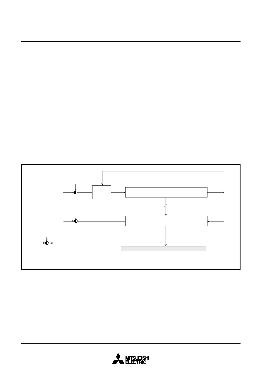
The M37210M3-XXXSP incorporates an interrupt interval determina-
tion circuit. This interrupt interval determination circuit has an 8-bit
binary up counter as shown in Figure 34.
Using this counter, it determines an interval or a pulse width on the
INT1 or INT2 (refer to Figure 36).
The following describes how the interrupt interval is determined.
1. The interrupt input to be determined (INT1 input or INT2 input) is
selected by using bit 2 in the interrupt interval determination con-
trol register (address 00D816). When this bit is cleared to “0”, the
INT1 input is selected ; when the bit is set to “1”, the INT2 input is
selected.
2. When the INT1 input is to be determined, the polarity is selected
by using bit 3 of the interrupt interval determination control regis-
ter ; when the INT2 input is to be determined, the polarity is se-
lected by using bit 4 of the interrupt interval determination control
register.
When the relevant bit is cleared to “0”, determination is made of
the interval of a positive polarity (rising transition) ; when the bit is
set to “1”, determination is made of the interval of a negative po-
Fig. 34 Block diagram of interrupt interval determination circuit
Note : The pulse width of external interrupt INT1 and INT2 needs 5 or more machine cycles.
Data bus
RE1
INT1
(Note)
RE0
RE2
INT2
32
s
8
8-bit binary up counter
Interrupt interval determination register
64
s
Address 00D716
Control
circuit
Selection gate : Connected to black
colored side at reset.
RE : Interrupt interval determination control register
larity (falling transition).
3. The reference clock is selected by using bit 1 of the interrupt inter-
val determination control register. When the bit is cleared to “0”, a
64
ms clock is selected ; when the bit is set to “1”, a 32
s clock is
selected (based on an oscillation frequency of 4MHz in either
case).
4. Simultaneously when the input pulse of the specified polarity (ris-
ing or falling transition) occurs on the INT1 pin (or INT2 pin), the 8-
bit binar y up counter starts counting up with the selected
reference clock (64
s or 32s).
5. Simultaneously with the next input pulse, the value of the 8-bit bi-
nary up counter is loaded into the determination register (address
00D716) and the counter is immediately reset (0016). The refer-
ence clock is input in succession even after the counter is reset,
and the counter restarts counting up from “0016”.
6. When count value “FE16” is reached, the 8-bit binary up counter
stops counting. Then, simultaneously when the next reference
clock is input, the counter sets value “FF16” to the determination
register.
相關(guān)PDF資料 |
PDF描述 |
|---|---|
| M37210M3-XXXSP | 8-BIT, MROM, 8.1 MHz, MICROCONTROLLER, PDIP52 |
| M37210E4SP | 8-BIT, OTPROM, 8.1 MHz, MICROCONTROLLER, PDIP52 |
| M37210M3-XXXFP | 8-BIT, MROM, 8.1 MHz, MICROCONTROLLER, PQFP64 |
| M37211M2-XXXSP | 8-BIT, MROM, 8.1 MHz, MICROCONTROLLER, PDIP52 |
| M37210E4-XXXSP | 8-BIT, OTPROM, 8.1 MHz, MICROCONTROLLER, PDIP52 |
相關(guān)代理商/技術(shù)參數(shù) |
參數(shù)描述 |
|---|---|
| M37210E4SP | 制造商:MITSUBISHI 制造商全稱:Mitsubishi Electric Semiconductor 功能描述:SINGLE-CHIP 8-BIT CMOS MICROCOMPUTER for VOLTAGE SYNTHESIZER with ON-SCREEN DISPLAY CONTROLLER |
| M37210E4-XXXFP | 制造商:RENESAS 制造商全稱:Renesas Technology Corp 功能描述:SINGLE-CHIP 8-BIT CMOS MICROCOMPUTER for VOLTAGE SYNTHESIZER with ON-SCREEN DISPLAY CONTROLLER |
| M37210E4-XXXSP | 制造商:RENESAS 制造商全稱:Renesas Technology Corp 功能描述:SINGLE-CHIP 8-BIT CMOS MICROCOMPUTER for VOLTAGE SYNTHESIZER with ON-SCREEN DISPLAY CONTROLLER |
| M37210M3 | 制造商:RENESAS 制造商全稱:Renesas Technology Corp 功能描述:SINGLE-CHIP 8-BIT CMOS MICROCOMPUTER for VOLTAGE SYNTHESIZER with ON-SCREEN DISPLAY CONTROLLER |
| M37210M3-010SP | 制造商:MITSUBISHI 制造商全稱:Mitsubishi Electric Semiconductor 功能描述:SINGLE-CHIP 8-BIT CMOS MICROCOMPUTER for VOLTAGE SYNTHESIZER with ON-SCREEN DISPLAY CONTROLLER |
發(fā)布緊急采購,3分鐘左右您將得到回復(fù)。