- 您現(xiàn)在的位置:買賣IC網(wǎng) > PDF目錄69014 > M37753M8C-XXXHP 16-BIT, MROM, 40 MHz, MICROCONTROLLER, PQFP80 PDF資料下載
參數(shù)資料
| 型號: | M37753M8C-XXXHP |
| 元件分類: | 微控制器/微處理器 |
| 英文描述: | 16-BIT, MROM, 40 MHz, MICROCONTROLLER, PQFP80 |
| 封裝: | FINE PITCH, QFP-80 |
| 文件頁數(shù): | 66/109頁 |
| 文件大小: | 865K |
| 代理商: | M37753M8C-XXXHP |
第1頁第2頁第3頁第4頁第5頁第6頁第7頁第8頁第9頁第10頁第11頁第12頁第13頁第14頁第15頁第16頁第17頁第18頁第19頁第20頁第21頁第22頁第23頁第24頁第25頁第26頁第27頁第28頁第29頁第30頁第31頁第32頁第33頁第34頁第35頁第36頁第37頁第38頁第39頁第40頁第41頁第42頁第43頁第44頁第45頁第46頁第47頁第48頁第49頁第50頁第51頁第52頁第53頁第54頁第55頁第56頁第57頁第58頁第59頁第60頁第61頁第62頁第63頁第64頁第65頁當(dāng)前第66頁第67頁第68頁第69頁第70頁第71頁第72頁第73頁第74頁第75頁第76頁第77頁第78頁第79頁第80頁第81頁第82頁第83頁第84頁第85頁第86頁第87頁第88頁第89頁第90頁第91頁第92頁第93頁第94頁第95頁第96頁第97頁第98頁第99頁第100頁第101頁第102頁第103頁第104頁第105頁第106頁第107頁第108頁第109頁
MITSUBISHI MICROCOMPUTERS
M37753M8C-XXXFP, M37753M8C-XXXHP
M37753S4CFP, M37753S4CHP
6
PRELIMINAR
Y
Notice:
This
is not
a final
specification.
Some
parametric
limits
are
subject
to change.
SINGLE-CHIP 16-BIT CMOS MICROCOMPUTER
BASIC FUNCTION BLOCKS
The M37753M8C-XXXFP and M37753M8C-XXXHP contain the fol-
lowing devices on single chips: ROM, RAM, CPU, bus interface unit,
timers, UART, A-D converter, D-A converter, I/O ports, clock gener-
ating circuit and others. Each of these devices is described below.
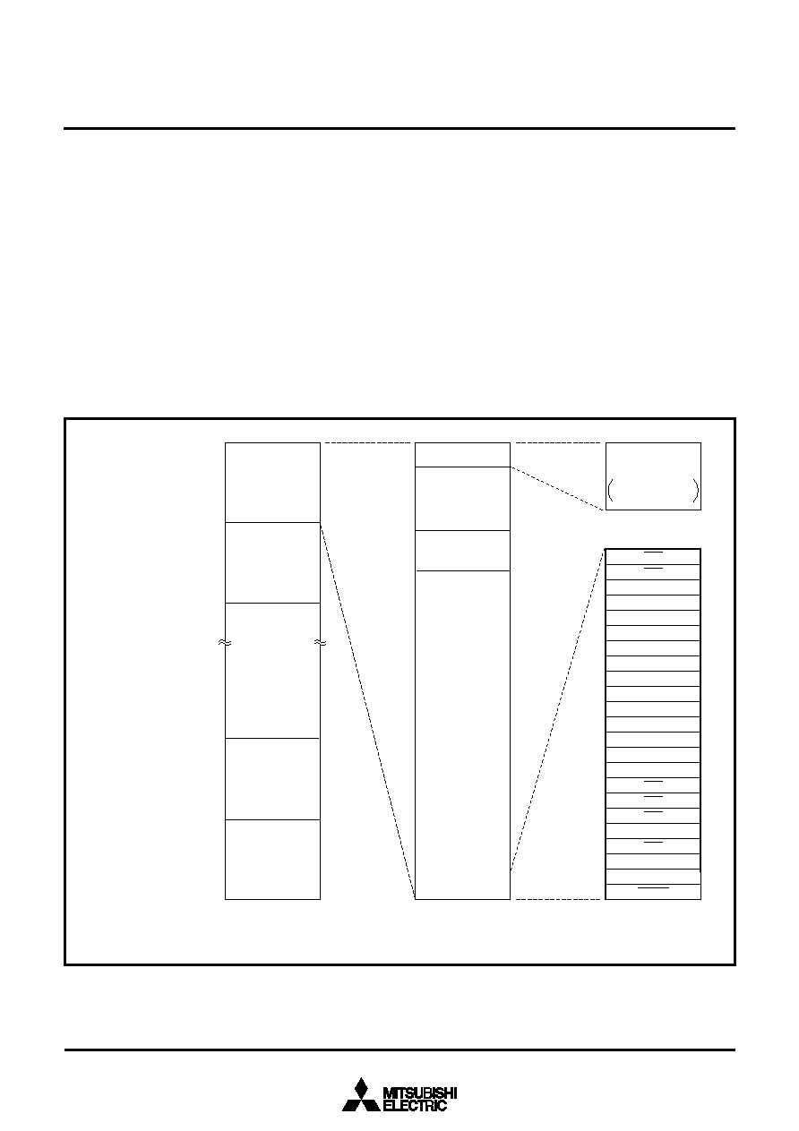
MEMORY
The memory map is shown in Figure 1. The address space is 16
Mbytes from addresses 016 to FFFFFF16. The address space is di-
vided into 64-Kbyte units called banks. The banks are numbered
from 016 to FF16.
Internal ROM, internal RAM, and control registers for internal periph-
eral devices are assigned to bank 016.
The 60-Kbyte area from addresses 100016 to FFFF16 is the internal
ROM.
Addresses FFD216 to FFFF16 are the RESET and interrupt vector
addresses and contain the interrupt vectors. Refer to the section on
interrupts for details.
The 2048-byte area from addresses 8016 to 87F16 contains the in-
ternal RAM. In addition to storing data, the RAM is used as stack dur-
ing a subroutine call, or interrupts.
Assigned to addresses 016 to 7F16 are peripheral devices such as
I/O ports, A-D converter, D-A converter, UART, timer, and interrupt
control registers.
Additionally the internal ROM area can be modified by software.
Refer to the section on ROM area modification function for details.
A 256-byte direct page area can be allocated anywhere in bank 016
using the direct page register DPR. In direct page addressing mode,
the memory in the direct page area can be accessed with two words
thus reducing program steps.
Note: Internal ROM area can be modified. (Refer to the section on ROM area modification function.)
00000016
00007F16
00087F16
00FFFF16
00FFFE16
00FFD216
00008016
00FFFF16
Bank 016
Bank 116
01000016
01FFFF16
FF000016
FFFFFF16
Internal RAM
2048 bytes
Peripherai devices
control registers
Interrupt vector table
A–D
INT3
UART1 transmit
UART1 receive
UART0 transmit
UART0 receive
Timer B2
Timer B1
Timer B0
Timer A4
Timer A3
Timer A2
Timer A1
Timer A0
INT2
Watchdog timer
BRK instruction
Zero divide
see Fig. 2 for
further information
INT1
INT0
DBC
RESET
Bank FF16
Internal ROM
60 Kbytes
00100016
FE000016
FEFFFF16
Bank FE16
00007F16
INT4
Fig. 1 Memory map
相關(guān)PDF資料 |
PDF描述 |
|---|---|
| M37754M6C-XXXGP | 16-BIT, MROM, 40 MHz, MICROCONTROLLER, PQFP100 |
| M37795STJ | 16-BIT, 8 MHz, MICROCONTROLLER, PQCC84 |
| M37795SJ | 16-BIT, 8 MHz, MICROCONTROLLER, PQCC84 |
| M37903S4CHP | 16-BIT, 26 MHz, MICROCONTROLLER, PQFP100 |
| M37920FCCHP | 16-BIT, FLASH, 20 MHz, MICROCONTROLLER, PQFP100 |
相關(guān)代理商/技術(shù)參數(shù) |
參數(shù)描述 |
|---|---|
| M37753S4CFP | 制造商:RENESAS 制造商全稱:Renesas Technology Corp 功能描述:SINGLE-CHIP 16-BIT CMOS MICROCOMPUTER |
| M37753S4CHP | 制造商:RENESAS 制造商全稱:Renesas Technology Corp 功能描述:SINGLE-CHIP 16-BIT CMOS MICROCOMPUTER |
| M37754 | 制造商:MITSUBISHI 制造商全稱:Mitsubishi Electric Semiconductor 功能描述:SINGLE-CHIP 16BIT CMOS MICROCOMPUTER |
| M37754FFCGP | 制造商:MITSUBISHI 制造商全稱:Mitsubishi Electric Semiconductor 功能描述:SINGLE-CHIP 16-BIT CMOS MICROCOMPUTER FLASH MEMORY VERSION |
| M37754FFCHP | 制造商:MITSUBISHI 制造商全稱:Mitsubishi Electric Semiconductor 功能描述:SINGLE-CHIP 16-BIT CMOS MICROCOMPUTER FLASH MEMORY VERSION |
發(fā)布緊急采購,3分鐘左右您將得到回復(fù)。