- 您現(xiàn)在的位置:買賣IC網(wǎng) > PDF目錄45043 > M38207M8-XXXFP 8-BIT, MROM, 4 MHz, MICROCONTROLLER, PQFP80 PDF資料下載
參數(shù)資料
| 型號(hào): | M38207M8-XXXFP |
| 元件分類: | 微控制器/微處理器 |
| 英文描述: | 8-BIT, MROM, 4 MHz, MICROCONTROLLER, PQFP80 |
| 封裝: | 0.80 MM PITCH, PLASTIC, QFP-80 |
| 文件頁數(shù): | 53/69頁 |
| 文件大小: | 944K |
| 代理商: | M38207M8-XXXFP |
第1頁第2頁第3頁第4頁第5頁第6頁第7頁第8頁第9頁第10頁第11頁第12頁第13頁第14頁第15頁第16頁第17頁第18頁第19頁第20頁第21頁第22頁第23頁第24頁第25頁第26頁第27頁第28頁第29頁第30頁第31頁第32頁第33頁第34頁第35頁第36頁第37頁第38頁第39頁第40頁第41頁第42頁第43頁第44頁第45頁第46頁第47頁第48頁第49頁第50頁第51頁第52頁當(dāng)前第53頁第54頁第55頁第56頁第57頁第58頁第59頁第60頁第61頁第62頁第63頁第64頁第65頁第66頁第67頁第68頁第69頁
Rev.4.01
Nov 14, 2003
page 57 of 136
3803/3804 Group
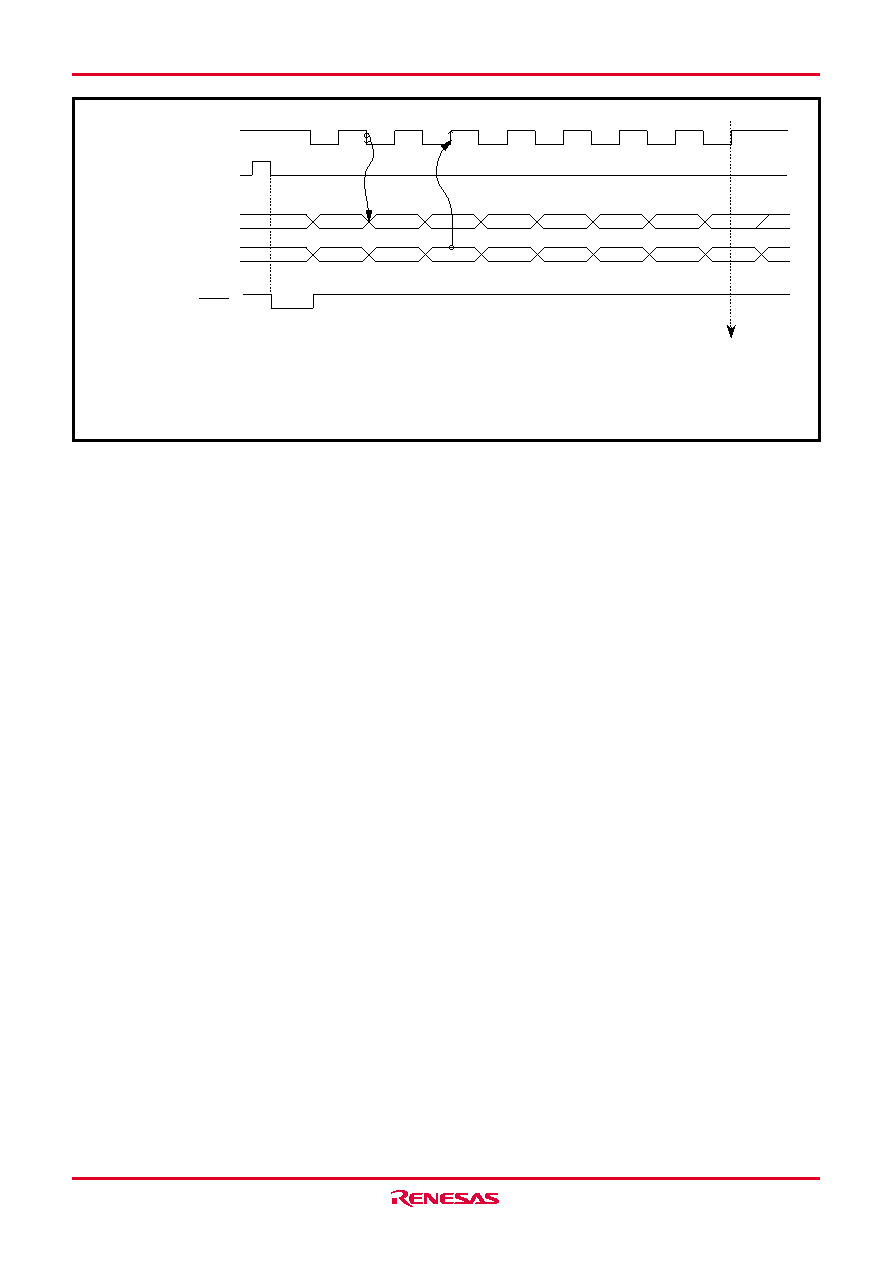
Fig. 47 Timing of serial I/O2
D7
D0
D1
D2
D3
D4
D5
D6
Transfer clock (Note 1)
Serial I/O2 output SOUT2
Serial I/O2 input SIN2
Receive enable signal SRDY2
Serial I/O2 register
write signal
(Note 2)
Serial I/O2 interrupt request bit set
1: When the internal clock is selected as the transfer clock, the divide ratio of f(XIN), or f(XCIN) in low-speed mode, can be
selected by setting bits 0 to 2 of the serial I/O2 control register.
2: When the internal clock is selected as the transfer clock, the SOUT2 pin goes to high impedance after transfer completion.
Notes
相關(guān)PDF資料 |
PDF描述 |
|---|---|
| M38203E4FS | 8-BIT, UVPROM, 4 MHz, MICROCONTROLLER, CQCC80 |
| M38203M4LXXXFP | 8-BIT, MROM, 4 MHz, MICROCONTROLLER, PQFP80 |
| M38207E8GP | 8-BIT, OTPROM, 4 MHz, MICROCONTROLLER, PQFP80 |
| M38207E8GP | 8-BIT, OTPROM, 4 MHz, MICROCONTROLLER, PQFP80 |
| M38203M4DXXXFP | 8-BIT, MROM, 4 MHz, MICROCONTROLLER, PQFP80 |
相關(guān)代理商/技術(shù)參數(shù) |
參數(shù)描述 |
|---|---|
| M38207RFS | 制造商:Renesas Electronics Corporation 功能描述:EMULATION MCU/8BIT CMOS EMULATION CHIP - Bulk |
| M3821 BK001 | 制造商:Alpha Wire 功能描述:CBL 25COND 18AWG BLK 1000' |
| M3821 BK002 | 制造商:Alpha Wire 功能描述:CBL 25COND 18AWG BLK 500' |
| M3821 BK005 | 制造商:Alpha Wire 功能描述:CBL 25COND 18AWG BLK 100' |
| M38220E1DFP | 制造商:MITSUBISHI 制造商全稱:Mitsubishi Electric Semiconductor 功能描述:SINGLE-CHIP 8-BIT CMOS MICROCOMPUTER |
發(fā)布緊急采購,3分鐘左右您將得到回復(fù)。