- 您現(xiàn)在的位置:買(mǎi)賣(mài)IC網(wǎng) > PDF目錄45048 > M38C89MF-XXXFP 8-BIT, MROM, 4 MHz, MICROCONTROLLER, PQFP144 PDF資料下載
參數(shù)資料
| 型號(hào): | M38C89MF-XXXFP |
| 元件分類(lèi): | 微控制器/微處理器 |
| 英文描述: | 8-BIT, MROM, 4 MHz, MICROCONTROLLER, PQFP144 |
| 封裝: | 20 X 20 MM, 0.50 MM PITCH, PLASTIC, LQFP-144 |
| 文件頁(yè)數(shù): | 25/55頁(yè) |
| 文件大小: | 981K |
| 代理商: | M38C89MF-XXXFP |
第1頁(yè)第2頁(yè)第3頁(yè)第4頁(yè)第5頁(yè)第6頁(yè)第7頁(yè)第8頁(yè)第9頁(yè)第10頁(yè)第11頁(yè)第12頁(yè)第13頁(yè)第14頁(yè)第15頁(yè)第16頁(yè)第17頁(yè)第18頁(yè)第19頁(yè)第20頁(yè)第21頁(yè)第22頁(yè)第23頁(yè)第24頁(yè)當(dāng)前第25頁(yè)第26頁(yè)第27頁(yè)第28頁(yè)第29頁(yè)第30頁(yè)第31頁(yè)第32頁(yè)第33頁(yè)第34頁(yè)第35頁(yè)第36頁(yè)第37頁(yè)第38頁(yè)第39頁(yè)第40頁(yè)第41頁(yè)第42頁(yè)第43頁(yè)第44頁(yè)第45頁(yè)第46頁(yè)第47頁(yè)第48頁(yè)第49頁(yè)第50頁(yè)第51頁(yè)第52頁(yè)第53頁(yè)第54頁(yè)第55頁(yè)
30
SINGLE-CHIP 8-BIT CMOS MICROCOMPUTER
MITSUBISHI MICROCOMPUTERS
38C8 Group
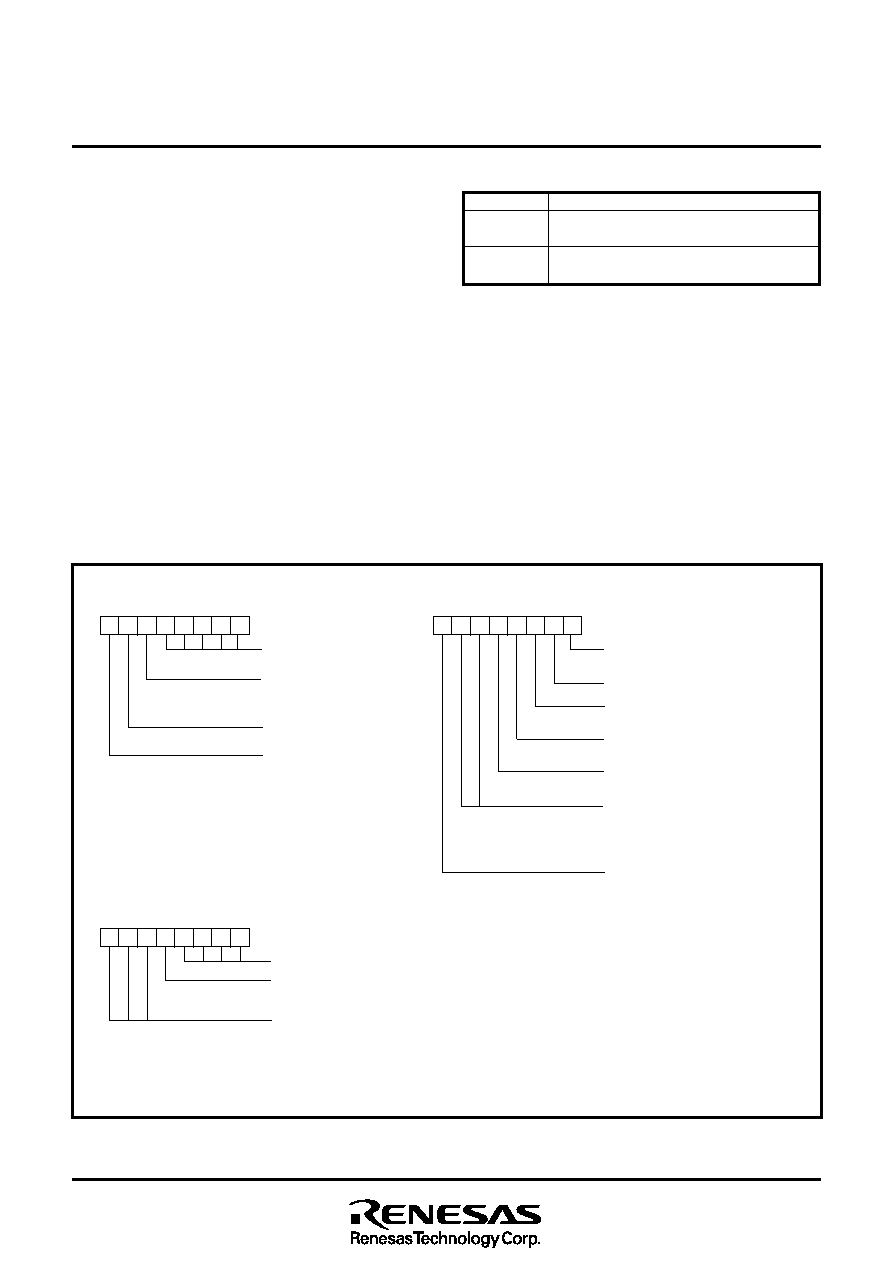
Fig. 28 Structure of LCD control register
Table 7 Maximum number of display pixels at each duty ratio
Duty ratio
Maximum number of display pixel
16 68 dots
(5 7 dots + cursor 2 lines)
32 52 dots
(5 7 dots + cursor 4 lines)
16
32
LCD Controller/Driver Function
The controller/driver performs the bias control and the time sharing
control by the LCD control registers 1, 2 (LC1, LC2), and the LCD
mode register (LM). The data of corresponding LCDRAM is output
from the segment pins according to the output timing of the common
pins.
The 38C8 group has the voltage multiplier only for LCD in addition to
LCD controller/driver .
[LCD mode register (LM)] 003916
The LCD mode register is used for setting the LCD controller/driver
according to the LCD panel used.
[LCD control register 1 (LC1)] 003716
The LCD control register 1 controls the voltage multiplier and built-in
resistance.
[LCD control register 2 (LC2)] 003816
The LCD control register 2 is write-only. Setting “1” to bit 5 makes
built-in resistance low resistance, and can raise drivability of the seg-
ment pins and the common pins.
Note: When executing the STP instruction while operating LCD, ex-
ecute the STP instruction after prohibiting LCD (set “0” to bit 3
of the LCD mode regsiter).
LCD control register 1
(LC1: address 003716)
b7
b0
Note 1: Consumption current can be reduced by restraint of drivability. But
an irregular display might be caused according to the panel or the
display pattern.
Not used (Do not write “1” to these bits.)
b7
b0
Note 2: The drive of a more large-scale LCD panel becomes easy by setting “1”
to this bit. But consumption current is increased at LCD drive. When
the drivability selection bit 1 is “1”, this function is invaid.
b7
b0
Note 3: LCDCK is a clock for a LCD timing controller.
Internal clock
φ is XCIN divided by 2 in the low-speed mode.
When selecting 32 duty, functions of pins 135 to 142 become COM16 to COM23,
and functions of pins 75 to 82 become COM24 to COM31.
Not used
(Do not write “1” to these bits.)
Duty ratio selsection bit
1 : 32 duty (use COM0–COM31)
0 : 16 duty (use COM0–COM15)
Not used
(Do not write “0” to this bit.)
LCD display RAM address selection bit
0 : 3 page
1 : 0 page
LCD enable bit
0 : LCD OFF
1 : LCD ON
LCD drive timing selection bit
0 : A type
1 : B type
LCDCK division ratio selection bits
b6 b5
0 0 : Clock input
0 1 : 2 division of clock input
1 0 : 4 division of clock input
1 1 : 8 division of clock input
LCDCK count source selection bit (Note 3)
0 : f(XIN)/1024
1 : f(XCIN)/16
LCD mode register
(LM: address 003916)
Voltage multiplier enable bit
0 : Voltage multiplier stop
1 : Voltage multiplier operating
Not used
(Do not write “1” to this bit.)
Drivability selection bit 1
0 : Normal (Drivability selection
bit 2 valid)
1 : Restraint (Note 1)
LCD control register 2
(LC2: address 003816)
Not used (Do not write “1” to these bits.)
Drivability selection bit 2
0 : Normal
1 : Reinforcing (Note 2)
相關(guān)PDF資料 |
PDF描述 |
|---|---|
| M38C89EFFP | 8-BIT, OTPROM, 4 MHz, MICROCONTROLLER, PQFP144 |
| M38D24G6HP | 8-BIT, FLASH, 6.25 MHz, MICROCONTROLLER, PQFP64 |
| M38D24G4FP | 8-BIT, FLASH, 6.25 MHz, MICROCONTROLLER, PQFP64 |
| M38D24G4-XXXHP | 8-BIT, FLASH, 6.25 MHz, MICROCONTROLLER, PQFP64 |
| M38D28G8HP | 8-BIT, FLASH, 6.25 MHz, MICROCONTROLLER, PQFP64 |
相關(guān)代理商/技術(shù)參數(shù) |
參數(shù)描述 |
|---|---|
| M38D20F1XXXFP | 制造商:RENESAS 制造商全稱(chēng):Renesas Technology Corp 功能描述:SINGLE-CHIP 8-BIT CMOS MICROCOMPUTER |
| M38D20F1XXXHP | 制造商:RENESAS 制造商全稱(chēng):Renesas Technology Corp 功能描述:SINGLE-CHIP 8-BIT CMOS MICROCOMPUTER |
| M38D20F2XXXFP | 制造商:RENESAS 制造商全稱(chēng):Renesas Technology Corp 功能描述:SINGLE-CHIP 8-BIT CMOS MICROCOMPUTER |
| M38D20F2XXXHP | 制造商:RENESAS 制造商全稱(chēng):Renesas Technology Corp 功能描述:SINGLE-CHIP 8-BIT CMOS MICROCOMPUTER |
| M38D20F3XXXFP | 制造商:RENESAS 制造商全稱(chēng):Renesas Technology Corp 功能描述:SINGLE-CHIP 8-BIT CMOS MICROCOMPUTER |
發(fā)布緊急采購(gòu),3分鐘左右您將得到回復(fù)。