- 您現在的位置:買賣IC網 > PDF目錄359066 > M48T37YMH (意法半導體) TRANS PREBIASED DUAL NPN SOT363 PDF資料下載
參數資料
| 型號: | M48T37YMH |
| 廠商: | 意法半導體 |
| 英文描述: | TRANS PREBIASED DUAL NPN SOT363 |
| 中文描述: | 3.3 - 5V的256千位的32KB的SRAM x8計時器 |
| 文件頁數: | 4/20頁 |
| 文件大?。?/td> | 128K |
| 代理商: | M48T37YMH |

M48T37Y, M48T37V
4/20
The memory locations, to provide user accessible
BYTEWIDE
clock information are in the bytes
with addresses 7FF1 and 7FF9h-7FFFh (located
in Table 11). The clock locations contain the cen-
tury, year, month, date, day, hour, minute, and
second in 24hour BCD format. Corrections for 28,
29 (leap year-compliant until the year 2100), 30,
and 31 day months are made automatically.
Byte 7FF8h is the clock control register. This byte
controls user access to the clock information and
also stores the clock calibration setting.
Byte 7FF7h contains the watchdog timer setting.
The watchdog timer redirects an out-of-control mi-
croprocessor and provides a reset orinterrupt to it.
Byte 7FF2h-7FF5h are reserved for clock alarm
programming.
These bytes can be used to set the alarm. This will
generate an active low signal on the IRQ/FT pin
when the alarm bytes match the date, hours, min-
utes and seconds of the clock. The eight clock
bytes are not the actual clock counters them-
selves; theyare memory locations consistingof Bi-
PORT
read/write memory cells. The M48T37Y/
37V includes a clock control circuit which updates
the clock bytes with current information once per
second. The information can be accessed by the
user in the same manner as any other location in
the staticmemory array.
The M48T37Y/37V also has itsown Power-failDe-
tect circuit. The control circuitry constantly moni-
tors the single V
CC
supply for an out of tolerance
condition. When V
CC
is out of tolerance, the circuit
writes protects the SRAM, providing a high degree
of data security in the midst of unpredictable sys-
tem operation broughton by low V
CC
. As V
CC
falls
below the Battery Back-up Switchover Voltage
(V
SO
), the control circuitry connects the battery
which maintainsdata and clock operation until val-
id power returns.
READ MODE
The M48T37Y/37V isin the Read Modewhenever
Write Enable (W) is high and Chip Enable (E) is
low. The unique address specified by the 15 Ad-
dressInputs defineswhichone of the32,752 bytes
of data is to be accessed. Valid data will be avail-
able at the Data I/O pins within Address Access
time (t
AVQV
) after the last address input signal is
stable, providing that the E and Output Enable (G)
access times are also satisfied. If the E and G ac-
cess times are not met, valid data will be available
after the latter of the Chip Enable Access time
(t
ELQV
) or Output Enable Access time (t
GLQV
).
The state of the eight three-state Data I/O signals
is controlled by E and G. If the outputs are activat-
ed before t
AVQV
, the data lineswill be driven to an
indeterminate state until t
AVQV
.
If the Address Inputs are changed while E and G
remain active, output data will remainvalid forOut-
put Data Hold time (t
AXQX
) but will be indetermi-
nate until the next Address Access.
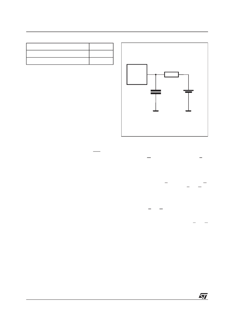
Table 4. AC Measurement Conditions
Note that Output Hi-Z is defined as the point where datais no longer
driven.
Input Rise and Fall Times
≤
5ns
Input Pulse Voltages
0 to 3V
Input and Output Timing Ref. Voltages
1.5V
Figure 4. AC Testing Load Circuit
Note: Excluding open-drain output pins.
AI02325
CL= 100pF
CLincludes JIG capacitance
645
DEVICE
UNDER
TEST
1.75V
相關PDF資料 |
PDF描述 |
|---|---|
| M48T37Y-70MH6TR | TRANS PREBIASED DUAL PNP SOT-363 |
| M48T37Y-70MH6 | TRANS PREBIAS DUAL COMP SOT-563 |
| M48T37Y-70MH1TR | TRANS PREBIASED DUAL COMP SOT363 |
| M48T37Y-10MH6TR | TRANS PREBIASED DUAL COMP SOT363 |
| M48T37Y-10MH6 | TRANS PREBIASED DUAL COMP SOT363 |
相關代理商/技術參數 |
參數描述 |
|---|---|
| M48T37YSH | 制造商:STMICROELECTRONICS 制造商全稱:STMicroelectronics 功能描述:3.3V-5V 256 Kbit 32Kb x8 TIMEKEEPER SRAM |
| M48T39Y | 制造商:STMICROELECTRONICS 制造商全稱:STMicroelectronics 功能描述:256 Kb 32K x8 TIMEKEEPER SRAM |
| M48T39Y-100PM1 | 制造商:STMICROELECTRONICS 制造商全稱:STMicroelectronics 功能描述:256 Kb 32K x8 TIMEKEEPER SRAM |
| M48T39Y-150PM1 | 制造商:STMICROELECTRONICS 制造商全稱:STMicroelectronics 功能描述:256 Kb 32K x8 TIMEKEEPER SRAM |
| M48T39YPM | 制造商:STMICROELECTRONICS 制造商全稱:STMicroelectronics 功能描述:256 Kb 32K x8 TIMEKEEPER SRAM |
發(fā)布緊急采購,3分鐘左右您將得到回復。