- 您現(xiàn)在的位置:買賣IC網(wǎng) > PDF目錄377830 > M52D32162A-7.5BG (ELITE SEMICONDUCTOR MEMORY TECHNOLOGY INC) 1M x 16Bit x 2Banks Synchronous DRAM PDF資料下載
參數(shù)資料
| 型號(hào): | M52D32162A-7.5BG |
| 廠商: | ELITE SEMICONDUCTOR MEMORY TECHNOLOGY INC |
| 元件分類: | DRAM |
| 英文描述: | 1M x 16Bit x 2Banks Synchronous DRAM |
| 中文描述: | 2M X 16 SYNCHRONOUS DRAM, 7 ns, PBGA54 |
| 封裝: | 8 X 8 MM, LEAD FREE, VFBGA-54 |
| 文件頁(yè)數(shù): | 11/30頁(yè) |
| 文件大小: | 784K |
| 代理商: | M52D32162A-7.5BG |
第1頁(yè)第2頁(yè)第3頁(yè)第4頁(yè)第5頁(yè)第6頁(yè)第7頁(yè)第8頁(yè)第9頁(yè)第10頁(yè)當(dāng)前第11頁(yè)第12頁(yè)第13頁(yè)第14頁(yè)第15頁(yè)第16頁(yè)第17頁(yè)第18頁(yè)第19頁(yè)第20頁(yè)第21頁(yè)第22頁(yè)第23頁(yè)第24頁(yè)第25頁(yè)第26頁(yè)第27頁(yè)第28頁(yè)第29頁(yè)第30頁(yè)
ES MT
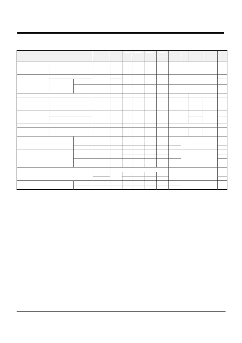
SIMPLIFIED TRUTH TABLE
M52D32162A
Elite Semiconductor Memory Technology Inc.
Publication Date
:
May. 2007
Revision
:
1.4
11/30
COMMAND
CKEn-1
CKEn
CS
RAS
CAS
WE
DQM BA A10/AP
A11,
A9~A0
Note
Mode Register Set
Extended Mode Register
Set
Auto Refresh
H
H
X
X
L
L
L
L
L
L
L
L
X
X
OP CODE
OP CODE
1,2
1,2
Register
H
L
3
3
3
3
4
Entry
H
L
L
L
H
X
X
L
H
L
H
X
L
H
X
H
H
X
H
Refresh
Self Refresh
Exit
L
H
X
X
Bank Active & Row Addr.
H
X
X
V
Row Address
L
Auto Precharge Disable
Read &
Column Address
Auto Precharge Enable
Auto Precharge Disable
H
X
L
H
L
H
X
V
H
L
H
Column
Address
(A0~A7)
Column
Address
(A0~A7)
4,5
4
Write & Column
Address
Burst Stop
Auto Precharge Enable
H
X
L
H
L
L
X
V
4,5
H
X
L
H
H
L
X
X
6
4
4
7
Bank Selection
Both Banks
V
X
L
H
Precharge
H
X
L
L
H
L
X
X
H
L
X
H
L
H
L
X
V
X
X
H
X
V
X
X
H
H
X
X
V
X
X
H
X
V
X
V
X
X
H
X
V
Entry
H
L
X
Clock Suspend or
Active Power Down
Exit
L
H
X
X
Entry
H
L
X
Precharge Power Down Mode
Exit
L
H
X
X
DQM
H
H
H
H
L
V
X
H
L
L
X
X
H
H
X
X
H
L
X
No Operation Command
X
X
X
Entry
Exit
L
H
X
X
Deep Power Down Mode
X
(V= Valid, X= Don’t Care, H= Logic High , L = Logic Low)
Note:
1. OP Code: Operation Code
A0~ A11/AP, BA: Program keys.(@MRS). BA=0 for MRS and BA=1 for EMRS.
2. MRS/EMRS can be issued only at both banks precharge state.
A new command can be issued after 2 clock cycle of MRS.
3. Auto refresh functions are as same as CBR refresh of DRAM.
The automatical precharge without row precharge command is meant by “Auto”.
Auto / self refresh can be issued only at both banks precharge state.
4. BA: Bank select address.
If “Low”: at read, write, row active and precharge, bank A is selected.
If “High”: at read, write, row active and precharge, bank B is selected.
If A10/AP is “High” at row precharge, BA ignored and both banks are selected.
5. During burst read or write with auto precharge, new read/write command can not be issued.
Another bank read /write command can be issued after the end of burst.
New row active of the associated bank can be issued at t
RP
after the end of burst.
6. Burst stop command is valid at every burst length.
7. DQM sampled at positive going edge of a CLK masks the data-in at the very CLK (Write DQM latency is 0), but
makes
Hi-Z state the data-out of 2 CLK cycles after. (Read DQM latency is 2)
相關(guān)PDF資料 |
PDF描述 |
|---|---|
| M52D32162A-7.5TG | 1M x 16Bit x 2Banks Synchronous DRAM |
| M52D32321A | 512K x 32Bit x 2Banks Synchronous DRAM |
| M52D32321A-10BG | 512K x 32Bit x 2Banks Synchronous DRAM |
| M52D32321A-7.5BG | 512K x 32Bit x 2Banks Synchronous DRAM |
| M52S128168A | 1M x 16 Bit x 4 Banks Synchronous DRAM |
相關(guān)代理商/技術(shù)參數(shù) |
參數(shù)描述 |
|---|---|
| M52D32162A-7BG | 制造商:ESMT 制造商全稱:Elite Semiconductor Memory Technology Inc. 功能描述:1M x 16Bit x 2Banks Mobile Synchronous DRAM |
| M52D32162A-7TG | 制造商:ESMT 制造商全稱:Elite Semiconductor Memory Technology Inc. 功能描述:1M x 16Bit x 2Banks Mobile Synchronous DRAM |
| M52D32321A | 制造商:ESMT 制造商全稱:Elite Semiconductor Memory Technology Inc. 功能描述:512K x 32Bit x 2Banks Mobile Synchronous DRAM |
| M52D32321A_09 | 制造商:ESMT 制造商全稱:Elite Semiconductor Memory Technology Inc. 功能描述:512K x 32Bit x 2Banks Mobile Synchronous DRAM |
| M52D32321A-10BG | 制造商:ESMT 制造商全稱:Elite Semiconductor Memory Technology Inc. 功能描述:512K x 32Bit x 2Banks Mobile Synchronous DRAM |
發(fā)布緊急采購(gòu),3分鐘左右您將得到回復(fù)。