- 您現(xiàn)在的位置:買賣IC網(wǎng) > PDF目錄370967 > M54977P (Mitsubishi Electric Corporation) Bi-CMOS 12-BIT SERIAL-INPUT LATCHED DRIVER PDF資料下載
參數(shù)資料
| 型號(hào): | M54977P |
| 廠商: | Mitsubishi Electric Corporation |
| 英文描述: | Bi-CMOS 12-BIT SERIAL-INPUT LATCHED DRIVER |
| 中文描述: | 雙CMOS 12位串行輸入鎖存驅(qū)動(dòng) |
| 文件頁數(shù): | 1/6頁 |
| 文件大小: | 500K |
| 代理商: | M54977P |

Bi-CMOS 12-BIT SERIAL-INPUT LATCHED DRIVER
M54977P
MITSUBISHI <CONTROL / DRIVER IC>
20
17
18
19
1
4
3
2
16
5
15
6
14
7
13
8
12
9
11
10
DESCRIPTION
The M54977P is a semiconductor integrated circuit fabricated
using Bi-CMOS technology. It contains a serial input to
serial/parallel output 12-bit CMOS shift register and CMOS latch as
well as bipolar 12-bit parallel-output driver.
FEATURES
G
Serial input to serial/parallel output
G
Cascade connections possible through serial output
G
Latch circuit included for each stage
G
Enable input for output control
G
Low supply current .................................. I
CC
≥
10
μ
A at standby
G
Serial input/output level is compatible with standard CMOS
G
Driver : Withstand voltage ...................................... BV
CEO
≥
30V
Large drive current ................................ (I
O(max)
=200mA)
G
Wide operating temperature range ..................... T
a
=-20 – +75
°
C
APPLICATION
Thermal printer head dot driver, Serial-to parallel conversion,
Relay, solenoid driver
FUNCTION
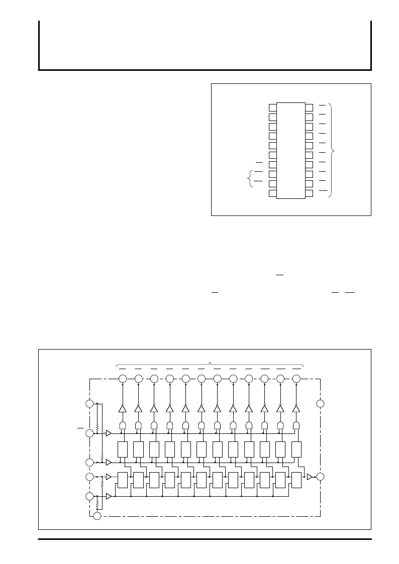
The M54977P consists of an 12-bit D-type flip-flop, the output of
which is connected to 12 latches.
When data is applied to the serial data input (S-IN) and a clock
pulse is applied to clock input (T), an “L” to “H” change of the clock
will cause the data input signals to enter the internal shift registers
and the data in the shift registers will be shifted in order.
Using a number of M54977P units for bit expansion in series will
entail connecting serial output (S-OUT) to S-IN of the next-stage
M54977P.
In parallel output, when the latch input is set to “H” and the output-
control input (enable input EN) is “L”, a clock pulse changing from
“L” to “H” will cause the serial data input signal to appear at output
O1, and the data will be shifted in order at outputs O2 – O12.
The parallel output will yield a signal that is inverted with respect to
the serial data input.
BLOCK DIAGRAM
PIN CONFIGURATION (TOP VIEW)
←
→
→
→
→
→
→
→
→
→
→
→
→
T
S-IN
L-GND
V
CC
S-OUT
LATCH
EN
P-GND
O1
O2
O3
O4
O5
O6
O7
O8
Clock
Serial input
Logic GND
Serial output
Latch input
Enable input
Driver GND
Parallel outputs
Outline 20P4
M
→
→
O9
O10
←
O12
←
O11
Parallel outputs
Q
L D
O1
20
Clock T
Q
T
D
Q
L D
O2
19
Q
T
D
Q
L D
O3
18
Q
T
D
Q
L D
O4
17
Q
T
D
Q
L D
O5
16
Q
T
D
Q
L D
O6
15
Q
T
D
Q
L D
O7
14
Q
T
D
Q
L D
O8
13
Q
T
D
Q
L D
O9
12
Q
T
D
Q
L D
O10
11
Q
T
D
Q
L D
O11
9
Q
T
D
Q
L D
O12
8
Q
T
D
EN
S-OUT
Serial output
P-GND
Driver GND
Parallel outputs
Power supply V
CC
Latch input
LATCH
Serial input
S-IN
Enable input
3
1
2
6
4
7
10
5
L-GND
相關(guān)PDF資料 |
PDF描述 |
|---|---|
| M54992 | Bi-CMOS 24-BIT SERIAL-INPUT LATCHED DRIVER |
| M54992FP | Bi-CMOS 24-BIT SERIAL-INPUT LATCHED DRIVER |
| M54992P | Bi-CMOS 24-BIT SERIAL-INPUT LATCHED DRIVER |
| M56754 | 4-CHANNEL ACTUATOR MOTOR DRIVER |
| M56754SP | 4-CHANNEL ACTUATOR MOTOR DRIVER |
相關(guān)代理商/技術(shù)參數(shù) |
參數(shù)描述 |
|---|---|
| M54992 | 制造商:MITSUBISHI 制造商全稱:Mitsubishi Electric Semiconductor 功能描述:Bi-CMOS 24-BIT SERIAL-INPUT LATCHED DRIVER |
| M54992FP | 制造商:MITSUBISHI 制造商全稱:Mitsubishi Electric Semiconductor 功能描述:Bi-CMOS 24-BIT SERIAL-INPUT LATCHED DRIVER |
| M54992P | 制造商:MITSUBISHI 制造商全稱:Mitsubishi Electric Semiconductor 功能描述:Bi-CMOS 24-BIT SERIAL-INPUT LATCHED DRIVER |
| M54995 | 制造商:MITSUBISHI 制造商全稱:Mitsubishi Electric Semiconductor 功能描述:nullBi-CMOS 8-BIT SERIAL-INPUT LATCHED DRIVER |
| M54995FP | 制造商:MITSUBISHI 制造商全稱:Mitsubishi Electric Semiconductor 功能描述:nullBi-CMOS 8-BIT SERIAL-INPUT LATCHED DRIVER |
發(fā)布緊急采購,3分鐘左右您將得到回復(fù)。