- 您現(xiàn)在的位置:買賣IC網(wǎng) > PDF目錄370976 > M5M512R88DJ-12 (Mitsubishi Electric Corporation) 1048576-BIT (131072-WORD BY 8-BIT) CMOS STATIC RAM PDF資料下載
參數(shù)資料
| 型號(hào): | M5M512R88DJ-12 |
| 廠商: | Mitsubishi Electric Corporation |
| 英文描述: | 1048576-BIT (131072-WORD BY 8-BIT) CMOS STATIC RAM |
| 中文描述: | 1048576位(131072 - Word的8位)的CMOS靜態(tài)RAM |
| 文件頁(yè)數(shù): | 2/6頁(yè) |
| 文件大?。?/td> | 62K |
| 代理商: | M5M512R88DJ-12 |

M5M512R88DJ-10,-12,-15
1048576-BIT (131072-WORD BY 8-BIT) CMOS STATIC RAM
MITSUBISHI
ELECTRIC
MITSUBISHI LSIs
V
I(S)
=V
IL
other inpus=V
IH
or V
IL
Output-open(duty 100%)
V
I
= 0 ~ Vcc
V
I(S)
=V
IH
V
I/O
= 0 ~ Vcc
- 2.*
Operating temperature
V
cc
V
I
V
O
P
d
T
opr
T
stg(bias)
T
stg
V
V
V
mW
°C
- 2.0*
1000
0 ~ 70
- 10 ~ 85
- 65 ~ 150
Ta=25°C
2
Icc
S
H
L
L
L
W
X
L
H
H
OE
X
X
L
H
Mode
Non selection
Write
Read
Stand by
Active
Active
Active
ABSOLUTE MAXIMUM RATINGS
Parameter
Supply voltage
Input voltage
Output voltage
Power dissipation
Storage temperature
(bias)
Storage temperature
Symbol
Unit
Conditions
With respect to GND
Ratings
DQ
High-impedance
Din
Dout
High-impedance
*
Pulse width
≤
5ns, In case of DC: - 0.5V
DC ELECTRICAL CHARACTERISTICS
(
Ta=0 ~ 70
°C
, Vcc=3.3V ,unless otherwise noted)
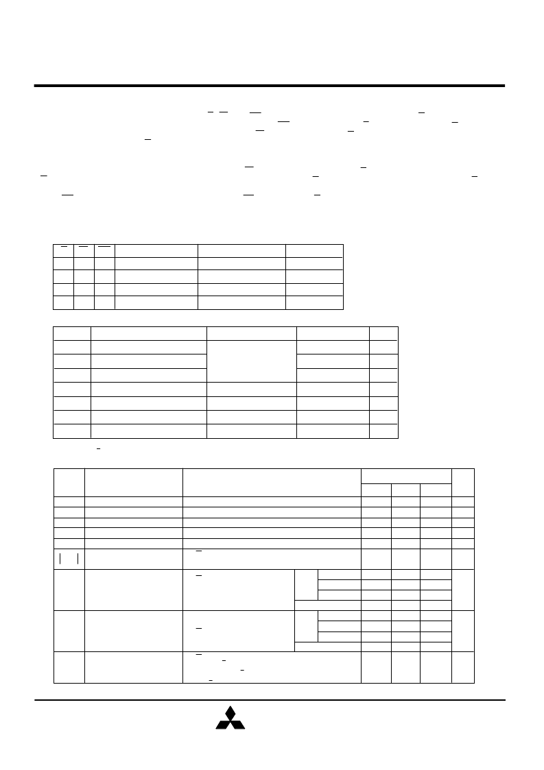
The operation mode of the M5M512R88DJ is determined by
a combination of the device control inputs S, W and OE.
Each mode is summarized in the function table.
A write cycle is executed whenever the low level W
overlaps with the low level S. The address must be set-up
before the write cycle and must be stable during the entire
cycle.
The data is latched into a cell on the trailing edge of W or
S, whichever occurs first, requiring the set-up and hold time
relative to these edge to be maintained. The output enable
input OE directly controls the output stage. Setting the OE at
a high level, the output stage is in a high impedance state,
and the data bus
contention problem in the write cycle is eliminated.
A read cycle is excuted by setting W at a high level and
OE at a low level while S are in an active state (S=L).
When setting S at high level, the chip is in a non-
selectable mode in which both reading and writing are
disable. In this mode, the output stage is in a high-
impedance state, allowing OR-tie with other chips and
memory expansion by S.
Signal-S controls the power-down feature. When S goes
high, power dissapation is reduced extremely. The access
time from S is equivalent to the address access time.
FUNCTION
- 2.0*
V
IH
V
IL
V
OH
V
OL
I
I
V
V
V
V
Vcc+0.3
0.8
2.0
2.4
0.4
I
OH
= - 4mA
I
OL
= 8mA
Symbol
Parameter
Max
Typ
Limits
Min
Condition
Unit
High-level input voltage
Low-level input voltage
High-level output voltage
Low-level output voltage
Input current
I
CC1
I
CC2
I
CC3
mA
mA
180
170
160
I
OZ
2
2
uA
uA
V
I(S)
=Vcc
≥
0.2V
other inputs V
I
≤
0.2V
or V
I
≥
Vcc - 0.2V
AC
DC
10
Active supply current
(TTL level)
Stand by current
(TTL level)
Output current in off-state
Stand by current
90
V
I(S)
=V
IH
FUNCTION TABLE
100
60
55
50
10ns cycle
12ns cycle
15ns cycle
mA
AC
DC
30
10ns cycle
12ns cycle
15ns cycle
- 5%
°C
°C
Note 1: Direction for current flowing into an IC is positive (no mark).
相關(guān)PDF資料 |
PDF描述 |
|---|---|
| M5M512R88DJ-15 | 1048576-BIT (131072-WORD BY 8-BIT) CMOS STATIC RAM |
| M5M51R16AWG-10HI | 1048576-BIT(65536-WORD BY 16-BIT)CMOS STATIC RAM |
| M5M51R16AWG-10LI | 1048576-BIT(65536-WORD BY 16-BIT)CMOS STATIC RAM |
| M5M51R16AWG-12HI | 1048576-BIT(65536-WORD BY 16-BIT)CMOS STATIC RAM |
| M5M51R16AWG-12LI | 1048576-BIT(65536-WORD BY 16-BIT)CMOS STATIC RAM |
相關(guān)代理商/技術(shù)參數(shù) |
參數(shù)描述 |
|---|---|
| M5M512R88DJ-15 | 制造商:MITSUBISHI 制造商全稱:Mitsubishi Electric Semiconductor 功能描述:1048576-BIT (131072-WORD BY 8-BIT) CMOS STATIC RAM |
| M5M514400D-60SJ | 制造商:OK International 功能描述: |
| M5M5165FP-10 | 制造商:MITSUBISHI 制造商全稱:Mitsubishi Electric Semiconductor 功能描述:65536-BIT (8192-WORD BY 8-BIT) CMOS STATIC RAM |
| M5M5165FP-10L | 制造商:MITSUBISHI 制造商全稱:Mitsubishi Electric Semiconductor 功能描述:65536-BIT (8192-WORD BY 8-BIT) CMOS STATIC RAM |
| M5M5165FP-12 | 制造商:MITSUBISHI 制造商全稱:Mitsubishi Electric Semiconductor 功能描述:65536-BIT (8192-WORD BY 8-BIT) CMOS STATIC RAM |
發(fā)布緊急采購(gòu),3分鐘左右您將得到回復(fù)。