- 您現(xiàn)在的位置:買賣IC網(wǎng) > PDF目錄370980 > M5M54R16ATP-15 (Mitsubishi Electric Corporation) 4194304-BIT (262144-WORD BY 16-BIT) CMOS STATIC RAM PDF資料下載
參數(shù)資料
| 型號(hào): | M5M54R16ATP-15 |
| 廠商: | Mitsubishi Electric Corporation |
| 英文描述: | 4194304-BIT (262144-WORD BY 16-BIT) CMOS STATIC RAM |
| 中文描述: | 4194304位(262144字由16位)的CMOS靜態(tài)RAM |
| 文件頁數(shù): | 1/7頁 |
| 文件大?。?/td> | 63K |
| 代理商: | M5M54R16ATP-15 |

M5M54R16AJ,ATP-10,-12,-15
MITSUBISHI LSIs
4194304-BIT (262144-WORD BY 16-BIT) CMOS STATIC RAM
MITSUBISHI
ELECTRIC
Fast access time M5M54R16AJ,ATP-10 ... 10ns(max)
M5M54R16AJ,ATP-12 ... 12ns(max)
M5M54R16AJ,ATP-15 ... 15ns(max)
Single +3.3V power supply
Fully static operation : No clocks, No refresh
Common data I/O
Easy memory expansion by S
Three-state outputs : OR-tie capability
OE prevents data contention in the I/O bus
Directly TTL compatible : All inputs and outputs
Separate control of lower and upper bytes by LB and UB
DESCRIPTION
The M5M54R16A is a family of 262144-word by 16-bit
static RAMs, fabricated with the high performance CMOS
process and designed for high speed application. These
devices operate on a single 3.3V supply, and are directly
TTL compatible.
They include a power down feature as well. In write
and read cycles, the lower and upper bytes are able
to be controled either togethe or separately by LB
and UB.
FEATURES
1
1998.11.30 Ver.B
PRELIMINARY
Notice: This is not a final specification.
Some parametric limits are subject to change.
APPLICATION
High-speed memory system
The operation mode of the M5M54R16A is determined
by a combination of the device control inputs S, W, OE,
LB, and UB. Each mode is summarized in the function
table.
A write cycle is executed whenever the low level W
overlaps with low level LB and/or low level UB and low
level S. The address must be set-up before write cycle
and must be stable during the entire cycle. which both reading and writing are enable, and upper-
The data is latched into a cell on the traling edge of
W, LB, UB or S, whichever occurs first, requiring the
set-up and hold time relative to these edge to be
maintained. The output enable input OE directly
controls the output stage. Setting the OE at a high level,
the output stage is in a high impedance state, and the
data bus contention problem in the write cycle is
eliminated.
A read cycle is excuted by setting W at a high level
and OE at a low level while LB and/or UB and S are in
an active
state. (LB and/or UB=L, S=L)
When setting LB at a high level and other pins are in
an active state, upper-Byte are in a selectable mode
in which both reading and writing are enable, and
lower-Byte are in a non-selectable mode. And when
setting UB at a high level and other pins are in an
active state, lower-Byte are in a selectable mode in
Byte are in a non-selectable mode.
When setting LB and UB at a high level or S at high
level, the chip is in a non-selectable mode in which
both reading and writing are disabled. In this mode,
the output stage is in a high-impedance state,
allowing OR-tie with other chips and memory
expansion by LB, UB and S.
Signal-S controls the power-down feature. When S
goes high, power dissapation is reduced extremely.
The access time from S is equivalent to the address
access time.
FUNCTION
PACKAGE
M5M54R16AJ .......... 44pin 400mil SOJ
M5M54R16ATP .......... 44pin 400mil TSOP(II)
Outline
44P0K
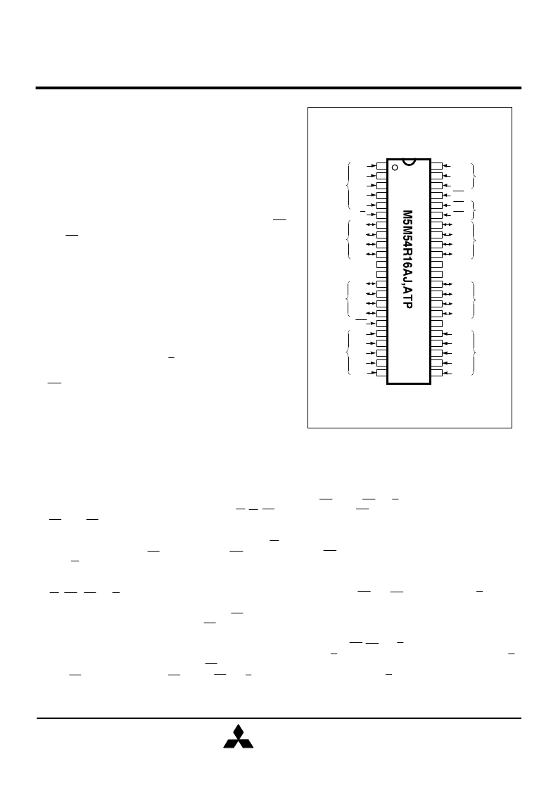
PIN CONFIGURATION (TOP VIEW)
1
2
3
4
5
6
7
8
9
10
11
12
13
14
15
16
DQ
1
DQ
2
DQ
3
GND
DQ
5
DQ
6
DQ
7
17
18
19
20
21
22
S
W
A
5
A
6
A
7
A
8
A
9
32
31
30
29
28
27
26
25
24
23
OE
UB
GND
V
CC
DQ
12
DQ
11
DQ
10
DQ
9
N.C
A
14
A
13
A
12
A
11
A
10
36
35
34
33
41
40
39
38
37
44
43
42
LB
DQ
16
DQ
15
DQ
14
DQ
13
ADDRESS
INPUTS
(3.3V)
(0V)
(3.3V)
(0V)
DATA
INPUTS/
OUTPUTS
DATA
INPUTS/
OUTPUTS
ADDRESS
INPUTS
ADDRESS
INPUTS
DATA
INPUTS/
OUTPUTS
DATA
INPUTS/
OUTPUTS
BYTE
CONTROL
INPUTS
A
0
A
1
A
2
A
3
A
4
A
17
A
16
A
15
DQ
4
V
CC
DQ
8
OUTPUT
ENABLE INPUT
ADDRESS
INPUTS
CHIP SELECT
INPUT
WRITE
CONTROL INPUT
相關(guān)PDF資料 |
PDF描述 |
|---|---|
| M5M564R16DJ-10 | 1048576-BIT (65536-WORD BY 16-BIT) CMOS STATIC RAM |
| M5M564R16DJ-12 | 1048576-BIT (65536-WORD BY 16-BIT) CMOS STATIC RAM |
| M5M564R16DJ-15 | 1048576-BIT (65536-WORD BY 16-BIT) CMOS STATIC RAM |
| M5M564R16DTP-15 | 1048576-BIT (65536-WORD BY 16-BIT) CMOS STATIC RAM |
| M5M564R16DTP-10 | 1048576-BIT (65536-WORD BY 16-BIT) CMOS STATIC RAM |
相關(guān)代理商/技術(shù)參數(shù) |
參數(shù)描述 |
|---|---|
| M5M564R16DJ-10 | 制造商:MITSUBISHI 制造商全稱:Mitsubishi Electric Semiconductor 功能描述:1048576-BIT (65536-WORD BY 16-BIT) CMOS STATIC RAM |
| M5M564R16DJ-12 | 制造商:MITSUBISHI 制造商全稱:Mitsubishi Electric Semiconductor 功能描述:1048576-BIT (65536-WORD BY 16-BIT) CMOS STATIC RAM |
| M5M564R16DJ-15 | 制造商:MITSUBISHI 制造商全稱:Mitsubishi Electric Semiconductor 功能描述:1048576-BIT (65536-WORD BY 16-BIT) CMOS STATIC RAM |
| M5M564R16DTP-10 | 制造商:MITSUBISHI 制造商全稱:Mitsubishi Electric Semiconductor 功能描述:1048576-BIT (65536-WORD BY 16-BIT) CMOS STATIC RAM |
| M5M564R16DTP-12 | 制造商:MITSUBISHI 制造商全稱:Mitsubishi Electric Semiconductor 功能描述:1048576-BIT (65536-WORD BY 16-BIT) CMOS STATIC RAM |
發(fā)布緊急采購,3分鐘左右您將得到回復(fù)。