- 您現(xiàn)在的位置:買賣IC網(wǎng) > PDF目錄370992 > M66503 (Mitsubishi Electric Corporation) 16-BIT CONSTANT CURRENT LED DRIVER with SHIFT REGISTER AND LATCH PDF資料下載
參數(shù)資料
| 型號: | M66503 |
| 廠商: | Mitsubishi Electric Corporation |
| 元件分類: | LED驅(qū)動器 |
| 英文描述: | 16-BIT CONSTANT CURRENT LED DRIVER with SHIFT REGISTER AND LATCH |
| 中文描述: | 16位恒流LED驅(qū)動器的移位寄存器和鎖存 |
| 文件頁數(shù): | 1/8頁 |
| 文件大小: | 114K |
| 代理商: | M66503 |

1
1616-BIT CONSTANT CURRENT LED DRIVER with SHIFT REGISTER AND LATCH
MIMITSUBISHI
DIDIGITAL ASSP
M66503ASP/AGP
DESCRIPTION
The M66503A is a constant current LED driver IC, whose
output current is variable. The IC’s functions include 16-bit
serial input/parallel output shift register with output latch.
The product uses Bi-CMOS process for highly accurate con-
stant current driving, permitting high-efficiency LED driving
without using a resistor that limits LED current.
Settings for the LED drive current are made by an external re-
sister, thereby ensuring a maximum output current of 30 mA,
enough for anode-common LED driving.
Furthermore, the pin configuration of the IC permits easier
wiring on a printed board.
FEATURES
Anode-common LED driving
Constant current output: Set to a value within a range be-
tween 0 and 30mA with an external resistor only.
Simultaneous lighting available.
Pins (OE
A
, OE
B
) provided for forced ON/OFF of LED drive
current.
Greater noise margin: Total-input Schmitt circuit is em-
ployed to deal with longer wire lengths.
Input/output CMOS compatible
Serial data output provided (SQ15)
5V single power supply
Pin configuration for easier wiring on printed board
APPLICATION
LED array drivers for display panel and printer. Other various
LED modules.
FUNCTION
The M66503A is a constant current LED driver for anode-
common LEDs. To set the LED driving current, an external
resistor is connected between the current setting input pin,
RC, and GND. In this way it is possible to set a highly accu-
rate drive current. Each bit of the shift register is made up of a
flip-flop performing shift function and a latch connected to the
output. When the clock input pin, CK
S
, goes from “L” to “H”,
data is shifted. Serial data is entered to the shift register via
the serial data input pin, A. Data on A is straight shifted. By
turning the latch enable input pin, LE, to “L”, the contents
stored in the shift register is latched. All outputs are turned off
if the output enable input pins, OE
A
and OE
B
, are simulta-
neously set to “L”. This function is useful for the prevention of
an excessive current flowing at the moment of power on. All
outputs are turned on if the OE
A
pin is set to “H”. This enables
to check LEDs for failure. In these actions, changing the state
of OE
A
and/or OE
B
does not affect the shift function. To ex-
pand the number of bits, link the M66503A in serial using the
serial data output pin, SQ15, which is the serial data output
of the shift register.
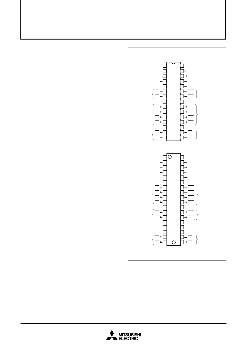
PIN CONFIGURATION (TOP VIEW)
1
2
3
4
5
6
7
8
9
GND1
M
Outline 30P4B
A
CK
S
LE
NC
Q
0
Q
1
GND2
Q
2
Q
3
Q
4
Q
5
10
11
12
13
14
15
GND3
Q
6
Q
7
30
29
28
27
26
25
24
23
22
21
20
19
18
17
16
V
CC
RC
SQ15
OE
A
OE
B
Q
15
Q
14
GND5
Q
13
Q
12
Q
11
Q
10
GND4
Q
9
Q
8
PARALLEL DATA
OUTPUT
Outline 36P2R-D
NC: No Connection
SERIAL DATA INPUT
SHIFT CLOCK INPUT
LATCH ENABLE
INPUT
SERIAL DATA INPUT
SHIFT CLOCK INPUT
LATCH ENABLE
INPUT
PARALLEL DATA
OUTPUT
PARALLEL DATA
OUTPUT
PARALLEL DATA
OUTPUT
PARALLEL DATA
OUTPUT
PARALLEL DATA
OUTPUT
PARALLEL DATA
OUTPUT
PARALLEL DATA
OUTPUT
PARALLEL DATA
OUTPUT
PARALLEL DATA
OUTPUT
PARALLEL DATA
OUTPUT
PARALLEL DATA
OUTPUT
CURRENT SETTING INPUT
SERIAL DATA OUTPUT
OUTPUT ENABLE INPUT A
OUTPUT ENABLE INPUT B
CURRENT SETTING INPUT
SERIAL DATA OUTPUT
OUTPUT ENABLE INPUT A
OUTPUT ENABLE INPUT B
36
35
34
33
32
31
30
29
28
27
26
25
24
23
22
21
20
19
M
1
2
3
4
5
6
7
8
9
10
11
12
13
14
15
16
17
18
A
CK
S
LE
NC
NC
Q
0
Q
1
Q
2
Q
3
GND2
Q
4
Q
5
NC
NC
NC
Q
6
Q
7
GND1
Q
9
Q
8
NC
NC
NC
Q
10
Q
11
GND3
Q
12
Q
15
Q
14
NC
OE
B
OE
A
SQ15
RC
V
CC
Q
13
相關(guān)PDF資料 |
PDF描述 |
|---|---|
| M66503AGP | 16-BIT CONSTANT CURRENT LED DRIVER with SHIFT REGISTER AND LATCH |
| M66503ASP | 16-BIT CONSTANT CURRENT LED DRIVER with SHIFT REGISTER AND LATCH |
| M66510 | LASER-DIODE DRIVER |
| M66510FP | LASER-DIODE DRIVER |
| M66510P | LASER-DIODE DRIVER |
相關(guān)代理商/技術(shù)參數(shù) |
參數(shù)描述 |
|---|---|
| M66503AGP | 制造商:MITSUBISHI 制造商全稱:Mitsubishi Electric Semiconductor 功能描述:16-BIT CONSTANT CURRENT LED DRIVER with SHIFT REGISTER AND LATCH |
| M66503ASP | 制造商:MITSUBISHI 制造商全稱:Mitsubishi Electric Semiconductor 功能描述:16-BIT CONSTANT CURRENT LED DRIVER with SHIFT REGISTER AND LATCH |
| M66510 | 制造商:MITSUBISHI 制造商全稱:Mitsubishi Electric Semiconductor 功能描述:LASER-DIODE DRIVER |
| M66510FP | 制造商:MITSUBISHI 制造商全稱:Mitsubishi Electric Semiconductor 功能描述:LASER-DIODE DRIVER |
| M66510P | 制造商:MITSUBISHI 制造商全稱:Mitsubishi Electric Semiconductor 功能描述:LASER-DIODE DRIVER |
發(fā)布緊急采購,3分鐘左右您將得到回復(fù)。