- 您現(xiàn)在的位置:買賣IC網(wǎng) > PDF目錄370992 > M66700P (Mitsubishi Electric Corporation) DUAL HIGH-SPEED CCD CLOCK DRIVER PDF資料下載
參數(shù)資料
| 型號: | M66700P |
| 廠商: | Mitsubishi Electric Corporation |
| 英文描述: | DUAL HIGH-SPEED CCD CLOCK DRIVER |
| 中文描述: | 雙高速CCD時鐘驅(qū)動器 |
| 文件頁數(shù): | 1/4頁 |
| 文件大小: | 71K |
| 代理商: | M66700P |

1
M66700P/WP
DUDUAL HIGH-SPEED CCD CLOCK DRIVER
M66700WP
Outline 16P4
1
2
3
4
8
7
6
5
Parameter
Supply voltage
Input voltage
Output voltage
Power dissipation
Storage temperature
Ratings
–0.5 ~ +15
–0.5 ~ +15
V
CC
950 (P) /1800 (WP)
–65 ~ 150
MIMITSUBISHI
DIDIGITAL ASSP
DESCRIPTION
M66700 Semiconductor Integrated Circuit is built in facsimi-
les and photocopiers to drive CCD linear image sensor data
transfer clocks at high speeds. Because this IC takes in data
on the TTL (Transistor-transistor logic) level, it can be driven
directly by a TTL integrated circuit.
FEATURES
Output logic amplitude: 12V
High-speed rise/fall time
t
r
= t
f
= 33ns (typical)
C
L
= 1000pF
High output “H” level voltage: (V
CC
– 1) V minimum
Low output “L” level voltage: 0.5V maximum
TTL input level
Package with improved allowable power dissipation (WP)
characteristic
APPLICATION
Driving of CCD image sensors in facsimiles, image scanners
and photocopiers
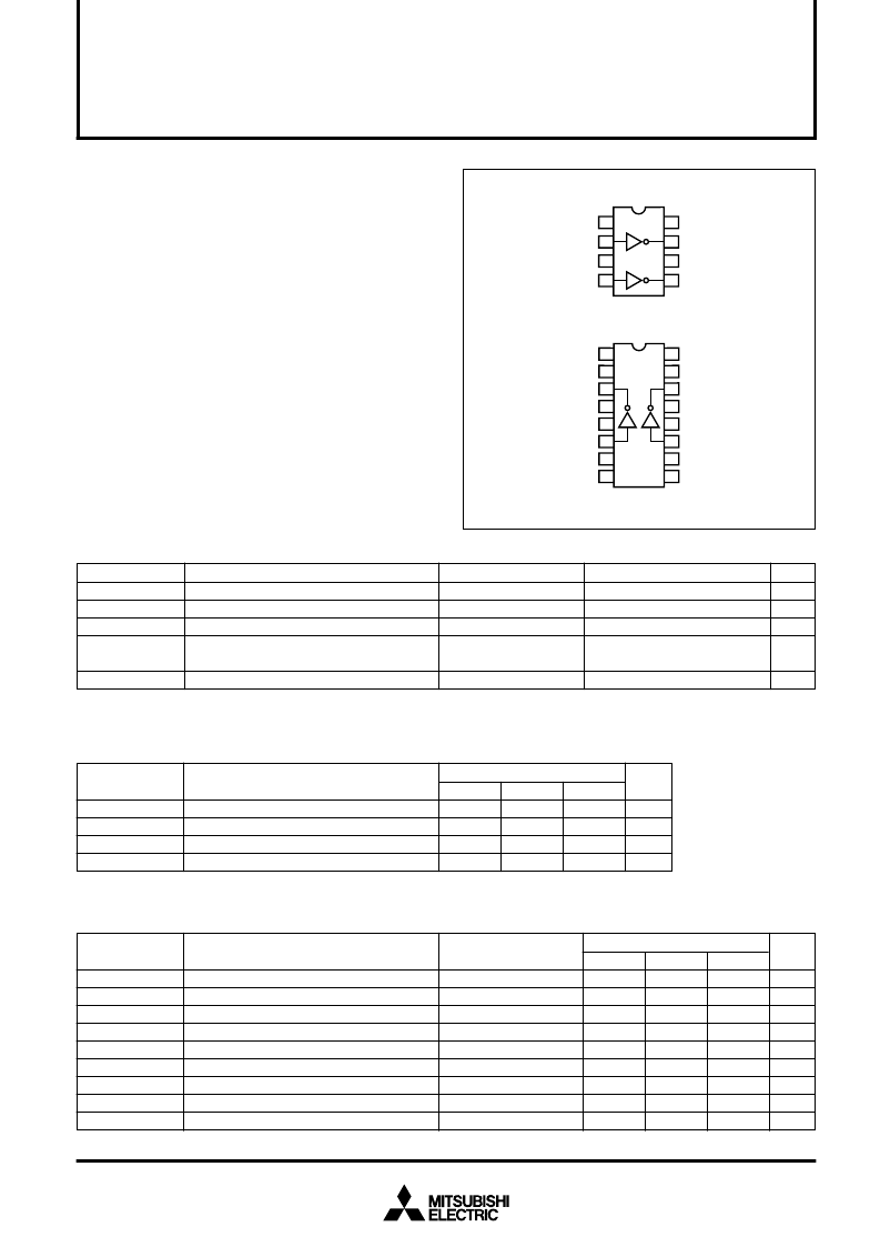
PIN CONFIGURATION (TOP VIEW)
Unit
V
V
V
mW
°
C
Symbol
V
CC
V
I
V
O
P
d
T
stg
Note 1: When T
a
is 25
°
C or higher, conduct derating as follows: 7.7mW/C
°
(P) /14.4mW/
°
C (WP).
ABSOLUTE MAXIMUM RATINGS
(T
a
= 0 ~ 70
°
C unless otherwise noted)
Conditions
Output: “H”
For single integrated
circuit;
T
a
= 25
°
C (Note 1)
NC: No Connection
←
→
OUTPUT
INPUT
V
CC
GND
OUTB
GND
GND
INB
GND
GND
INPUT
→
←
→
→
NC
OUTA
V
CC
OUTB
→
→
NC
INA
GND
INB
INPUT
INPUT
OUTPUT
OUTPUT
OUTPUT
RECOMMENDED OPERATIONAL CONDITIONS
Unit
V
V
V
°
C
Max.
13.2
0.8
70
Typ.
12.0
Min.
10.8
2.0
0
Parameter
Supply voltage
“H” input voltage
“L” input voltage
Operating temperature
Symbol
V
CC
V
IH
V
IL
T
opr
Limits
Limits
Typ.
(Note 2)
Test conditions
I
IC
= –18mA
V
I
= 0.4V, I
OH
= –1mA
V
I
= 2.0V, I
OL
= +1mA
V
I
= 5.5V
V
CC
= 12V, V
I
= 0.4V
V
CC
= 12V, V
I
= 0.0V
V
CC
= 12V, V
I
= 4.5V
Parameter
“H” input voltage
“L” input voltage
Input clamp voltage
“H” output voltage
“L” output voltage
“H” input current
“L” input current
“H” supply current
“L” supply current
Symbol
V
IH
V
IL
V
IC
V
OH
V
OL
I
IH
I
IL
I
CC H
I
CC L
Note 2: Standard values are measured under V
CC
= 12V and T
a
= 25
°
C.
ELECTRICAL CHARACTERISTICS
(V
CC
= 12V
±
10% and T
a
= 0 ~ 70
°
C unless otherwise noted)
Max.
0.8
–1.5
0.5
100
–0.4
5
38
Unit
V
V
V
V
V
μ
A
mA
mA
mA
–0.82
11.3
0.23
–0.13
2.2
29.2
Min.
2.0
V
CC
–
1
1
2
3
4
5
6
7
8
16
15
14
13
12
11
10
9
GND
GND
OUTA
GND
GND
INA
GND
GND
M66700P
Outline 8P4
相關PDF資料 |
PDF描述 |
|---|---|
| M66700WP | DUAL HIGH-SPEED CCD CLOCK DRIVER |
| M66701P | DUAL HIGH-SPEED CCD CLOCK DRIVER |
| M66851FP | SRAM TYPE FIFO MEMORY |
| M66850FP | SRAM TYPE FIFO MEMORY |
| M66850J | SRAM TYPE FIFO MEMORY |
相關代理商/技術參數(shù) |
參數(shù)描述 |
|---|---|
| M66700WP | 制造商:MITSUBISHI 制造商全稱:Mitsubishi Electric Semiconductor 功能描述:DUAL HIGH-SPEED CCD CLOCK DRIVER |
| M66701P | 制造商:MITSUBISHI 制造商全稱:Mitsubishi Electric Semiconductor 功能描述:DUAL HIGH-SPEED CCD CLOCK DRIVER |
| M668 | 制造商:未知廠家 制造商全稱:未知廠家 功能描述:DUAL TONE MELODY XMAS LIGHT CONTROL |
| M66850FP | 制造商:MITSUBISHI 制造商全稱:Mitsubishi Electric Semiconductor 功能描述:SRAM TYPE FIFO MEMORY |
| M66850J | 制造商:MITSUBISHI 制造商全稱:Mitsubishi Electric Semiconductor 功能描述:SRAM TYPE FIFO MEMORY |
發(fā)布緊急采購,3分鐘左右您將得到回復。