- 您現(xiàn)在的位置:買賣IC網(wǎng) > PDF目錄359088 > M68AF511AM70MC1T (意法半導(dǎo)體) 4 Mbit (512K x8), 5V Asynchronous SRAM PDF資料下載
參數(shù)資料
| 型號: | M68AF511AM70MC1T |
| 廠商: | 意法半導(dǎo)體 |
| 英文描述: | 4 Mbit (512K x8), 5V Asynchronous SRAM |
| 中文描述: | 4兆位(為512k × 8),5V的異步SRAM |
| 文件頁數(shù): | 11/18頁 |
| 文件大小: | 129K |
| 代理商: | M68AF511AM70MC1T |

11/18
M68AF511A
Write Mode
The M68AF511A is in the Write mode whenever
the W and E pins are Low. Either the Chip Enable
input (E) or the Write Enable input (W) must be de-
asserted during Address transitions for subse-
quent write cycles. Write begins with the concur-
rence of Chip Enable being active with W low.
Therefore, address setup time is referenced to
Write Enable and Chip Enable as t
AVWL
and t
AVEH
respectively, and is determined by the latter occur-
ring edge.
The Write cycle can be terminated by the earlier
rising edge of E, or W.
if the Output is enabled (E = Low and G = Low),
then W will return the outputs to high impedance
within t
WLQZ
of its falling edge. Care must be taken
to avoid bus contention in this type of operation.
Data input must be valid for t
DVWH
before the ris-
ing edge of Write Enable, or for t
DVEH
before the
rising edge of E, whichever occurs first, and re-
main valid for t
WHDX
or t
EHDX
.
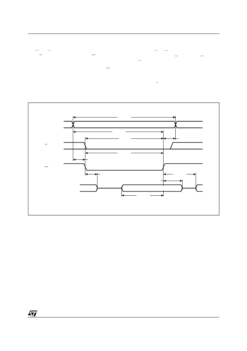
Figure 10. Write Enable Controlled, Write AC Waveforms
Note: 1. During this period DQ0-DQ7 are in output state and input signal should not be applied.
AI05913
tAVAV
tWHAX
tDVWH
DATA INPUT
A0-A18
E
W
DQ0-DQ7
VALID
tAVWH
tELWH
tWLWH
tAVWL
tWLQZ
tWHDX
tWHQX
DATA
(1)
DATA
(1)
相關(guān)PDF資料 |
PDF描述 |
|---|---|
| M68AW031A | CLAMP |
| M68AW031AL70MS6U | CLAMP |
| M68AW031AL70N6U | CLAMP |
| M68AW031AL70NS6U | CLAMP |
| M68AW031AM70MS6U | CAC 5C 5#16S SKT PLUG |
相關(guān)代理商/技術(shù)參數(shù) |
參數(shù)描述 |
|---|---|
| M68AF511AM70MC1U | 制造商:STMicroelectronics 功能描述: |
| M68AF511AM70MC6T | 制造商:STMicroelectronics 功能描述: |
| M68AF511AM70MC6U | 功能描述:RAM其它 WIRELESS FLASH RoHS:否 制造商:Freescale Semiconductor 封裝:Tray |
| M68AF511AM70NC1T | 制造商:STMICROELECTRONICS 制造商全稱:STMicroelectronics 功能描述:4 Mbit (512K x8), 5V Asynchronous SRAM |
| M68AF511AM70NC6 | 制造商:STMicroelectronics 功能描述: |
發(fā)布緊急采購,3分鐘左右您將得到回復(fù)。