11/18
M68AW511A
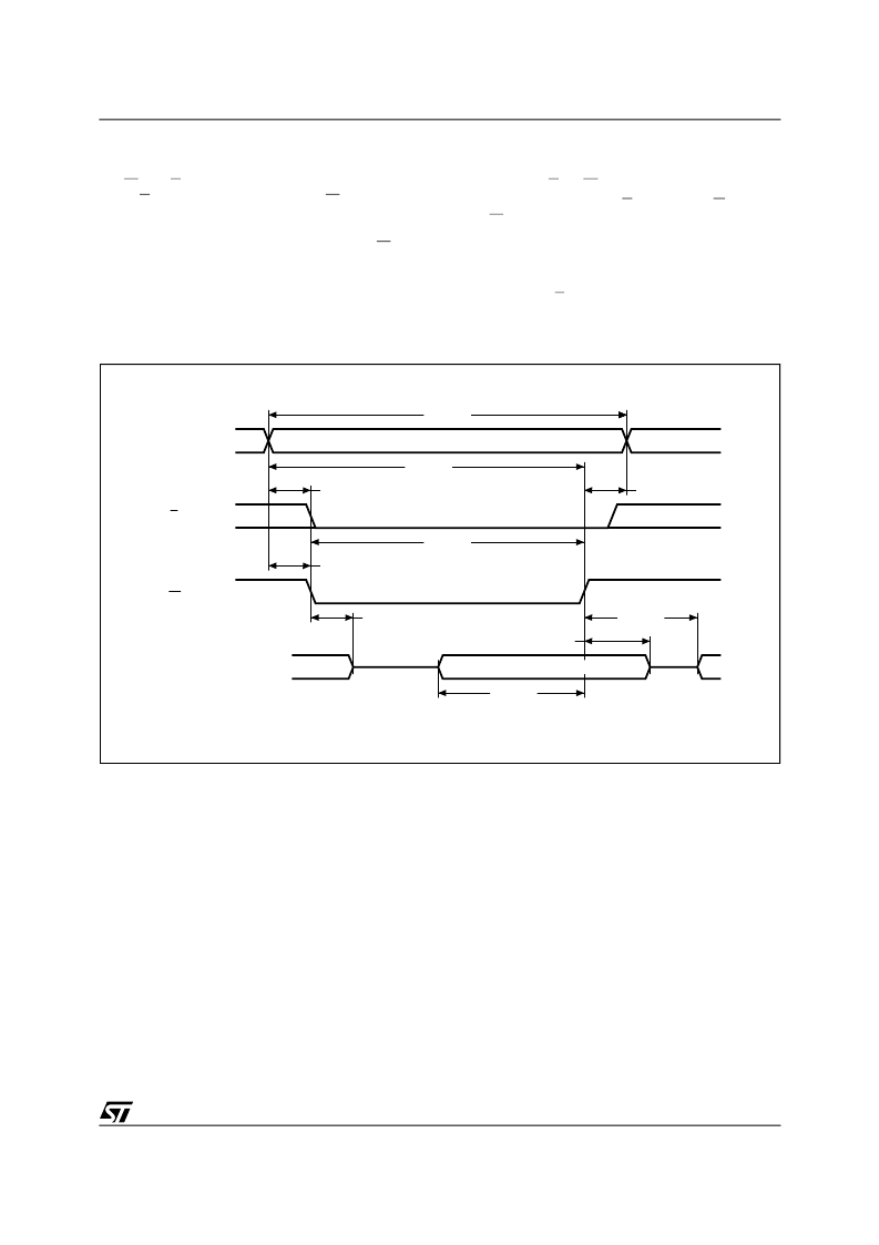
Write Mode
The M68AW511A is in the Write mode whenever
the W and E pins are Low. Either the Chip Enable
input (E) or the Write Enable input (W) must be de-
asserted during Address transitions for subse-
quent write cycles. Write begins with the concur-
rence of Chip Enable being active with W low.
Therefore, address setup time is referenced to
Write Enable and Chip Enable as t
AVWL
and t
AVEH
respectively, and is determined by the latter occur-
ring edge.
The Write cycle can be terminated by the earlier
rising edge of E, or W.
if the Output is enabled (E = Low and G = Low),
then W will return the outputs to high impedance
within t
WLQZ
of its falling edge. Care must be taken
to avoid bus contention in this type of operation.
Data input must be valid for t
DVWH
before the ris-
ing edge of Write Enable, or for t
DVEH
before the
rising edge of E, whichever occurs first, and re-
main valid for t
WHDX
or t
EHDX
.
Figure 10. Write Enable Controlled, Write AC Waveforms
AI03037
tAVAV
tWHAX
tDVWH
DATA INPUT
A0-A18
E
W
DQ0-DQ7
VALID
tAVWH
tAVEL
tWLWH
tAVWL
tWLQZ
tWHDX
tWHQX
