- 您現(xiàn)在的位置:買賣IC網 > PDF目錄359105 > M83530 (Littelfuse, Inc.) Varistor Products - Aerospace and Military PDF資料下載
參數(shù)資料
| 型號: | M83530 |
| 廠商: | Littelfuse, Inc. |
| 元件分類: | 壓敏電阻 |
| 英文描述: | Varistor Products - Aerospace and Military |
| 中文描述: | 壓敏電阻器產品-航天和軍事 |
| 文件頁數(shù): | 8/10頁 |
| 文件大小: | 78K |
| 代理商: | M83530 |

152
www.littelfuse.com
Varistor Products
Aerospace and Military
Neutron Effects
A second MOV-zener comparison was made in response to neutron
fluence.The selected devices were equal in area.
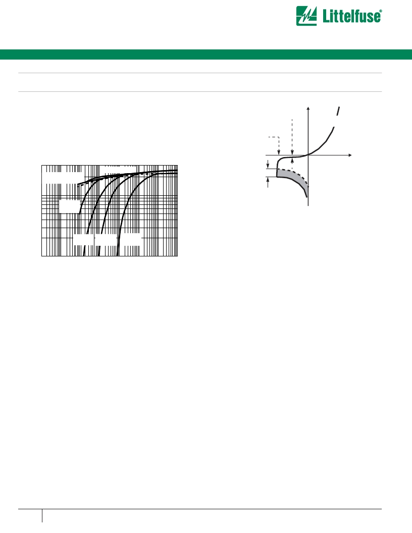
Figure 2 shows the clamping voltage response of the MOV and the zener
to neutron irradiation to as high as 10
15
N/cm
2
. It is apparent that in con-
trast to the large change in the zener, the MOV is unaltered. At higher-
currents where the MOV’s clamping voltage is again unchanged, the
zener device clamping voltage increases by as much as 36%.
At low reverse voltage, the device will conduct very little current (the
saturation current). At higher reverse voltage VBO(breakdown
voltage),the current increases rapidly as the electrons are either pulled
by the electric field (Zener effect) or knocked out by other electrons
(avalanching). A further increase in voltage causes the device to exhibit
a negative resistance characteristic leading to secondary breakdown.
This manifests itself through the formation of hotspots, and irreversible
damage occurs.This failure threshold decreases under neutron irradia-
tion for zeners, but not for Zinc Oxide Varistors.
Gamma Radiation
Radiation damage studies were performed on type V130LA2 varistors.
Emission spectra and V-I characteristics were collected before and after
irradiation with 10
6
rads Co
60
gamma radiation.
Both show no change, within experimental error, after irradiation.
Counterclockwise rotation of the V-I characteristics is observed in silicon
devices at high neutron irradiation levels; in other words, increasing
leakage at low current levels and increasing clamping voltage at higher
current levels.
The solid and open circles for a given fluence represent the high and low
breakdown currents for the sample of devices tested. Note that there is a
marked decrease in current (or energy) handling capability with
increased neutron fluence.
Failure threshold of silicon semiconductor junctions is further reduced
when high or rapidly increasing currents are applied. Junctions develop
hot spots, which enlarge until a short occurs if current is not limited or
quickly removed.
The characteristic voltage current relationship of a PN-Junction is shown
in Figure 3.
V
200
100
80
60
50
40
20
10
8
10
10
7
AMPERES
10
6
10
4
10
3
300
30
10
10
10
5
1.5K 200
AT 10
15
1.5K 200 INITIAL
VARISTOR V130A2
INITIAL AT 10
15
1.5K 200
AT 10
1.5K 200
AT 10
1.5K 200
AT 10
FIGURE 2. V-I CHARACTERISTIC RESPONSE TO NEUTRON
IRRADIATION FOR MOV AND ZENER DIODE
DEVICES
SATURATION
CURRENT
BREAKDOWN
VOLTAGE
I
V
REDUCTION IN
FAILURE STRESSHOLD
BY RADIAL
SECONDARY
BREAKDOWN
REVERSE
BIAS
FORWARD
BIAS
FIGURE 3. V-I CHARACTERISTIC OF PN-JUNCTION
High Reliability Varistors
相關PDF資料 |
PDF描述 |
|---|---|
| M83M83C | TRIPLE-BALANCED MIXER |
| M8438A | SERIAL INPUT LCD DRIVER |
| M8438AB6 | SERIAL INPUT LCD DRIVER |
| M8438AC6 | SERIAL INPUT LCD DRIVER |
| M8438ADIE1 | SERIAL INPUT LCD DRIVER |
相關代理商/技術參數(shù) |
參數(shù)描述 |
|---|---|
| M83530/1-2000B | 功能描述:壓敏電阻 M83530/1-2000B RoHS:否 制造商:EPCOS 產品:MLV 電壓額定值 DC:22 V 電壓額定值 AC:17 V 鉗位電壓:50 V 直徑: 峰值浪涌電流:30 A 浪涌能量額定值:75 mJ 電容:74.2 pF 工作溫度范圍:- 55 C to + 125 C 安裝:SMD/SMT 封裝:Reel |
| M83530/1-2200D | 功能描述:壓敏電阻 M83530/1-2200D RoHS:否 制造商:EPCOS 產品:MLV 電壓額定值 DC:22 V 電壓額定值 AC:17 V 鉗位電壓:50 V 直徑: 峰值浪涌電流:30 A 浪涌能量額定值:75 mJ 電容:74.2 pF 工作溫度范圍:- 55 C to + 125 C 安裝:SMD/SMT 封裝:Reel |
| M83530/1-4300E | 功能描述:壓敏電阻 M83530/1-4300E RoHS:否 制造商:EPCOS 產品:MLV 電壓額定值 DC:22 V 電壓額定值 AC:17 V 鉗位電壓:50 V 直徑: 峰值浪涌電流:30 A 浪涌能量額定值:75 mJ 電容:74.2 pF 工作溫度范圍:- 55 C to + 125 C 安裝:SMD/SMT 封裝:Reel |
| M83530/1-5100E | 功能描述:壓敏電阻 M83530/1-5100E RoHS:否 制造商:EPCOS 產品:MLV 電壓額定值 DC:22 V 電壓額定值 AC:17 V 鉗位電壓:50 V 直徑: 峰值浪涌電流:30 A 浪涌能量額定值:75 mJ 電容:74.2 pF 工作溫度范圍:- 55 C to + 125 C 安裝:SMD/SMT 封裝:Reel |
| M83531/01-001 | 制造商:Pulse 功能描述:LB10C9 - Rail/Tube |
發(fā)布緊急采購,3分鐘左右您將得到回復。