- 您現(xiàn)在的位置:買賣IC網(wǎng) > PDF目錄370998 > MAC7111VVF (Motorola, Inc.) Handheld Infrared Thermometer; Temperature Measuring Range:-20 C to 500 C; Response Time:500ms; Features:Laser Sighting; Accuracy: 1% PDF資料下載
參數(shù)資料
| 型號(hào): | MAC7111VVF |
| 廠商: | Motorola, Inc. |
| 英文描述: | Handheld Infrared Thermometer; Temperature Measuring Range:-20 C to 500 C; Response Time:500ms; Features:Laser Sighting; Accuracy: 1% |
| 中文描述: | MAC7100微控制器系列硬件規(guī)格 |
| 文件頁數(shù): | 28/48頁 |
| 文件大小: | 1514K |
| 代理商: | MAC7111VVF |
第1頁第2頁第3頁第4頁第5頁第6頁第7頁第8頁第9頁第10頁第11頁第12頁第13頁第14頁第15頁第16頁第17頁第18頁第19頁第20頁第21頁第22頁第23頁第24頁第25頁第26頁第27頁當(dāng)前第28頁第29頁第30頁第31頁第32頁第33頁第34頁第35頁第36頁第37頁第38頁第39頁第40頁第41頁第42頁第43頁第44頁第45頁第46頁第47頁第48頁

28
MAC7100 Microcontroller Family Hardware Specifications
PRELIMINARY—SUBJECT TO CHANGE WITHOUT NOTICE
For More Information On This Product,
Go to: www.freescale.com
MOTOROLA
Electrical Characteristics
3.10.4 ATD Timing Specifications
6
Maximum leakage occurs at maximum operating temperature. Current decreases by approximately one-half for
each 8 to 12
°
C, in the ambient temperature range of 50 to 125
°
C.
Below disruptive current conditions, the channel being stressed has conversion values of 0x3FF for analog inputs
greater than V
RH
and 0x000 for values less than V
RL
. This assumes that V
DD
A
≥
AV
RH
and V
RL
≥
V
SS
A due to the
presence of the sample amplifier. Other channels are not affected by non-disruptive conditions.
Coupling Ratio, K, is defined as the ratio of the output current, I
OUT
, measured on the pin under test to the injection
current, I
INJ
, when both adjacent pins are overstressed with the specified injection current. K = I
OUT
÷
I
INJ
. The input
voltage error on the channel under test is calculated as Verr = I
INJ
x K x R
S
.
Total injection current is determined by the number of channels injecting (for example, 15), external injection voltage
(V
INJ
– V
POSCLAMP
, or V
INJ
– V
NEGCLAMP
), and the external source impedance, Rs, wherein all input channels have
the same values. To determine the error voltage on the converted channel, only the two adjacent channels are
expected to contribute to the error voltage: V
errj
= (V
INJ
– V
CLAMP
)
×
K
×
2.
10
For a maximum sampling error of the input voltage
≤
1LSB, then the external filter capacitor, C
f
≥
1024
×
C
SAMP
. The
value of C
SAMP
in the new design may be reduced, or increased slightly.
7
8
9
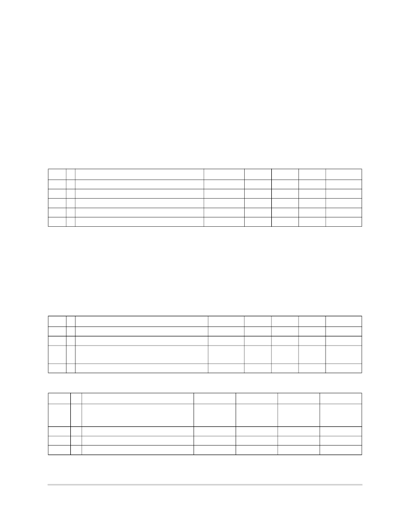
Table 30. ATD Performance Specifications
1
1
All voltages referred to V
SS
A, V
DD
A = 5.0 V±10%, ATD clock = 2.1 Mhz., –40 to 125
°
C.
Note: 1 LSB = 1 Count (At V
REF
= 5.12 V, one 8 bit count = 20 mV, one 10-bit count = 5 mV)
These values include quantization error which is inherently 1/2 count for any A/D converter.
This value is based on error attributed to the specified leakage value of TBD nA resulting in an error of less than 1/2
LSB (2.5 mV). If operating conditions are less than worst case or leakage-induced error is acceptable, larger values
of source resistance is allowable.
Num C
Rating
Symbol
Min
Typ
Max
Unit
T1
T2
T3
T4
T5
D 10-bit Resolution
D 10-bit Differential Nonlinearity
2
D 10-bit Integral Nonlinearity
2
D 10-bit Absolute Error
2, 3
D Max input Source Impedance
4
LSB
DNL
INL
AE
R
S
—
–1
–2
–2.5
—
5
—
—
—
—
—
1
2
2.5
100
mV
2
Counts
Counts
Counts
k
3
4
Table 31. ATD Timing Specifications
Num C
Rating
Symbol
Min
Typ
Max
Unit
U1
U2
U3
D ATD Module Clock Frequency
D ATD Conversion Clock Frequency
D ATD 10-bit Conversion Period
*
F
clk
F
atdclk
N
CONV10
*
T
CONV10
—
0.5
14
*
7
—
—
—
—
25.0
2.0
28
*
14
MHz
MHz
Cycles
*
μ
sec
Clock Cycles
Conv. Time
U4
D Stop Recovery Time (V
DD
A = 5.0 V)
T
SR
—
—
100
μ
sec
Table 32. ATD External Trigger Timing Specifications
Num
C
Parameter
Symbol
Min
Max
Unit
V1
D ETRIG Minimum Period
T
PERIOD
—
1 sample +
1 conv. +
1 ATD clock
—
—
2
CYCLE
V2
V3
V4
D ETRIG Minimum Pulse Width
D ETRIG Level Recovery
1
D Conversion Start Delay
t
PW
t
LR
t
DLY
2
1
—
SYS CLK
SYS CLK
SYS CLK
1
Time prior to end of conversion that the ETRIG pin must be deactivated so that another conversion sequence does
not start.
F
Freescale Semiconductor, Inc.
n
.
相關(guān)PDF資料 |
PDF描述 |
|---|---|
| MAC7121VVF | MAC7100 Microcontroller Family Hardware Specifications |
| MAC7131VVF | MAC7100 Microcontroller Family Hardware Specifications |
| MAC7141VVF | MAC7100 Microcontroller Family Hardware Specifications |
| MAC97-8 | CONVERTER DC-DC 20W 24V/5V DUAL |
| MAC97-4 | TRIACs 0.8 AMPERE RMS 200 - 600 VOLTS |
相關(guān)代理商/技術(shù)參數(shù) |
參數(shù)描述 |
|---|---|
| MAC7111VVF50 | 制造商:FREESCALE 制造商全稱:Freescale Semiconductor, Inc 功能描述:Microcontroller Family Hardware Specifications |
| MAC7111VVM50 | 制造商:FREESCALE 制造商全稱:Freescale Semiconductor, Inc 功能描述:Microcontroller Family Hardware Specifications |
| MAC7112 | 制造商:FREESCALE 制造商全稱:Freescale Semiconductor, Inc 功能描述:Microcontroller Family Reference Manual |
| MAC7112CAF50 | 制造商:FREESCALE 制造商全稱:Freescale Semiconductor, Inc 功能描述:Microcontroller Family Hardware Specifications |
| MAC7112CAG50 | 制造商:FREESCALE 制造商全稱:Freescale Semiconductor, Inc 功能描述:Microcontroller Family Hardware Specifications |
發(fā)布緊急采購,3分鐘左右您將得到回復(fù)。