- 您現(xiàn)在的位置:買賣IC網(wǎng) > PDF目錄383314 > MAX1233EGI (MAXIM INTEGRATED PRODUCTS INC) 【15kV ESD-Protected Touch-Screen Controllers Include DAC and Keypad Controller PDF資料下載
參數(shù)資料
| 型號: | MAX1233EGI |
| 廠商: | MAXIM INTEGRATED PRODUCTS INC |
| 元件分類: | 消費家電 |
| 英文描述: | 【15kV ESD-Protected Touch-Screen Controllers Include DAC and Keypad Controller |
| 中文描述: | SPECIALTY CONSUMER CIRCUIT, QCC28 |
| 封裝: | 5 X 5 MM, 0.80 MM HEIGHT, QFN-28 |
| 文件頁數(shù): | 29/44頁 |
| 文件大?。?/td> | 706K |
| 代理商: | MAX1233EGI |
第1頁第2頁第3頁第4頁第5頁第6頁第7頁第8頁第9頁第10頁第11頁第12頁第13頁第14頁第15頁第16頁第17頁第18頁第19頁第20頁第21頁第22頁第23頁第24頁第25頁第26頁第27頁第28頁當前第29頁第30頁第31頁第32頁第33頁第34頁第35頁第36頁第37頁第38頁第39頁第40頁第41頁第42頁第43頁第44頁
M
±15kV ESD-Protected Touch-Screen
Controllers Include DAC and Keypad Controller
______________________________________________________________________________________
29
DAC Data Register
The DAC data register stores data that is to be written
to the 8-bit DAC.
Table 36
shows the configuration of
the DAC data register. It is right justified with bit 7
–
bit 0
storing the input data.
GPIO Data Register
Tables 37
and
38
show the format and descriptions for
the GPIO data register. The register is left justified with
data in bit 15
–
bit 8. Reading the GPIO data register
gives the state of the R_ and C_ pins. Data written to
the GPIO data register appears on those R_ and C_
pins, which are configured as general-purpose outputs.
Data written to pins not configured as general-purpose
outputs is not stored.
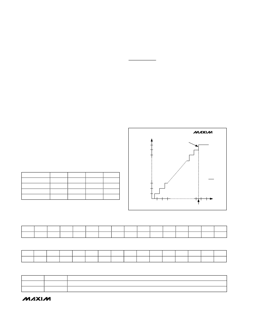
ADC Transfer Function
The MAX1233/MAX1234 output data is in straight bina-
ry format as shown in
Figure 11
. This
figure
shows the
ideal output code for the given input voltage and does
not include the effects of offset error, gain error, noise,
or nonlinearity.
Applications Information
Programmable 8-/10-/12-Bit Resolution
The MAX1233/MAX1234 provide the option of three dif-
ferent resolutions for the ADC: 8, 10, or 12 bits. Lower
resolutions are practical for some measurements such
as touch pressure. Lower resolution conversions have
smaller conversion times and therefore consume less
power. Program the resolution of the MAX1233/
MAX1234 12-bit ADCs by writing to the RES1 and RES0
bits in the ADC control register. When the MAX1233/
MAX1234 power up, both bits are set to zero so the
resolution is set to 8 bits with a 31μs internally timed
reference power-up delay as indicated by the ADC res-
olution control table. As explained in the control register
section, the RES1 and RES0 bits control the reference
COMPONENT
R1
R2
R3
R4
C1
K0
K1
K2
K3
C2
K4
K5
K6
K7
C3
K8
K9
K10
K11
C4
K12
K13
K14
K15
Table 35. Keypad to Key Bit Mapping
BIT15
0
BIT14
0
BIT13
0
BIT12
0
BIT11
0
BIT10
0
BIT9
0
BIT8
0
BIT7
DA7
BIT6
DA6
BIT5
DA5
BIT4
DA4
BIT3
DA3
BIT2
DA2
BIT1
DA1
BIT0
DA0
Table 36. DAC Data Register
BIT15
GPD7
BIT14
GPD6
BIT13
GPD5
BIT12
GPD4
BIT11
GPD3
BIT10
GPD2
BIT9
GPD1
BIT8
GPD0
BIT7
0
BIT6
0
BIT5
0
BIT4
0
BIT3
0
BIT2
0
BIT1
0
BIT0
0
Table 37. GPIO Data Register
BIT
15...8
7...0
NAME
GPD7...0
0
DESCRIPTION
GPIO data bits for GPIO pins 7...0
Reserved
Table 38. GPIO Data Register Descriptions
OUTPUT CODE
FULL-SCALE
TRANSITION
11 ... 111
11 ... 110
11 ... 101
00 ... 011
00 ... 010
00 ... 001
00 ... 000
3
0
FS
FS - 3/2LSB
FS = V
REF
ZS = GND
1LSB = V
INPUT VOLTAGE (LSB)
4096
2
1
MAX1233
MAX1234
Figure 11. Ideal Input Voltages and Output Codes
發(fā)布緊急采購,3分鐘左右您將得到回復。