- 您現在的位置:買賣IC網 > PDF目錄383325 > MAX1552ETE (MAXIM INTEGRATED PRODUCTS INC) Complete Power IC for Low-Cost PDAs PDF資料下載
參數資料
| 型號: | MAX1552ETE |
| 廠商: | MAXIM INTEGRATED PRODUCTS INC |
| 元件分類: | 電源管理 |
| 英文描述: | Complete Power IC for Low-Cost PDAs |
| 中文描述: | 1-CHANNEL POWER SUPPLY SUPPORT CKT, PQCC16 |
| 封裝: | 4 X 4 MM, 0.80 MM HEIGHT, MO-220, TQFN-16 |
| 文件頁數: | 9/12頁 |
| 文件大小: | 324K |
| 代理商: | MAX1552ETE |
and are commonly available in values up to 10μF. X7R
and X5R dielectrics are recommended. Note that some
ceramic dielectrics, such as Z5U and Y5V, exhibit large
capacitance and ESR variation with temperature and
require larger than the recommended values to main-
tain stability over temperature.
LCD Boost Output
Selecting an Inductor
The LCD boost is designed to operate with a wide range
of inductor values (4.7μH to 22μH). Smaller inductance
values typically offer smaller physical size for a given
series resistance or saturation current. Smaller values
make LX switch more frequently for a given load and
can reduce efficiency at low load currents. Larger val-
ues reduce switching losses due to less frequent
switching for a given load, but higher resistance may
then reduce efficiency. A 10μH inductor provides a
good balance and works well for most applications. The
inductor
’
s saturation current rating should be greater
than the peak switching current (250mA); however, it is
generally acceptable to bias some inductors into satura-
tion by as much as 20%, although this slightly reduces
efficiency.
Selecting a Diode
Schottky diodes rated at 250mA or more, such as the
Motorola MBRS0530 or Nihon EP05Q03L, are recom-
mended. The diode reverse-breakdown voltage rating
must be greater than the LCD output voltage.
Selecting Capacitors
For most applications, use a small 1μF LCD output
capacitor. This typically provides an output ripple of
30mV
P-P
. In addition, bypass IN with 1μF, and SW with
4.7μF ceramic capacitors.
An LCD feed-forward capacitor, connected from the
output to FB, improves stability over a wide range of
battery voltages. A 33pF capacitor is sufficient for most
applications; however, this value is also affected by PC
board layout.
Setting the LCD Voltage
Adjust the output voltage by connecting a voltage-
divider from the output (V
OUT
) to FB (see Figure 1).
Select R2 between 10k
and 200k
. Calculate R1 with
the following equation:
R1 = R2 [(V
OUT
/ V
FB
) - 1]
where V
FB
= 1.25V and V
OUT
can range from V
IN
to
28V. The input bias current of FB is typically only 5nA,
which allows large-value resistors to be used. For less
than 1% error, the current through R2 should be greater
than 100 times the feedback input bias current (I
FB
).
LCD Adjustment
The LCD boost output can be digitally adjusted by
either a DAC or PWM signal.
DAC Adjustment
Adding a DAC and a resistor, R
D,
to the divider circuit
(Figure 3) provides DAC adjustment of V
OUT
. Ensure
that V
OUT(MAX)
does not exceed the LCD panel rating.
The output voltage (V
OUT
) as a function of the DAC
voltage (V
DOUT
) can be calculated using the
following formula:
Using PWM Signals
Many microprocessors have the ability to create PWM
outputs. These are digital outputs, based on either 16-
bit or 8-bit counters, with programmable duty cycle. In
many applications they are suitable for adjusting the
output of the MAX1552 (Figure 1).
V
R
R
V
R
R
OUT
DOUT
D
1 25
×
.
)
×
=
+
+
(
1
1
2
1 25
1
M
Complete Power IC for
Low-Cost PDAs
_______________________________________________________________________________________
9
MAX1552
MAIN
COR1
SW
LCD OFF
SWITCH
LX
LFB
GND
LBO
IN
Li+
SWIN
REF
ON
OFF
0.1
μ
F
0.1
μ
F
ENSD
3.3V, 300mA
3.3V, 200mA
1.5V, 200mA
1.8V, 20mA
LCD
20V
1mA
ENC2
ENLCD
RESET OUT
LOW BATT OUT
RS
SDIG
COR2
TO MAIN
SDIG
COR2
LCD
ON
OFF
ON
OFF
LDO
CONTROL
LDO
CONTROL
LDO
CONTROL
LDO
CONTROL
LCD
BOOST
REF
THSD
BIAS
CURRENT
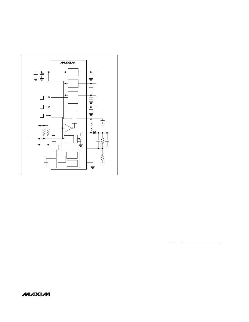
Figure 2. Block Diagram
相關PDF資料 |
PDF描述 |
|---|---|
| MAX1553ETA | High-Efficiency, 40V Step-Up Converters for 2 to 10 White LEDs |
| MAX1553EVKIT | MAX1553 Evaluation Kit |
| MAX1554ETA | High-Efficiency, 40V Step-Up Converters for 2 to 10 White LEDs |
| MAX1555EZK | PLASTIC ENCAPSULATED DEVICES |
| MAX1556ETB | 16レA IQ, 1.2A PWM Step-Down DC-DC Converters |
相關代理商/技術參數 |
參數描述 |
|---|---|
| MAX1552ETE-T | 功能描述:PMIC 解決方案 Complete PMIC for PDAs RoHS:否 制造商:Texas Instruments 安裝風格:SMD/SMT 封裝 / 箱體:QFN-24 封裝:Reel |
| MAX1552EVKIT | 制造商:Maxim Integrated Products 功能描述:COMPLETE PMIC FOR LOW COST PDA'S - Rail/Tube |
| MAX1553ETA | 制造商:Maxim Integrated Products 功能描述:SMALLEST, HIGHEST-EFFICIENCY, 40V STEP-UP CON - Rail/Tube 制造商:Rochester Electronics LLC 功能描述: |
| MAX1553ETA+ | 制造商:Maxim Integrated Products 功能描述:LED DRVR 10SEGMENT 2.7V TO 5.5V 8TDFN EP - Rail/Tube |
| MAX1553ETA+T | 功能描述:LED照明驅動器 40V StepUp Converter for 2-10 White LEDs RoHS:否 制造商:STMicroelectronics 輸入電壓:11.5 V to 23 V 工作頻率: 最大電源電流:1.7 mA 輸出電流: 最大工作溫度: 安裝風格:SMD/SMT 封裝 / 箱體:SO-16N |
發(fā)布緊急采購,3分鐘左右您將得到回復。