- 您現(xiàn)在的位置:買賣IC網(wǎng) > PDF目錄9863 > MAX3454EEUD+T (Maxim Integrated Products)IC TXRX USB ESD-PROT 14TSSOP PDF資料下載
參數(shù)資料
| 型號: | MAX3454EEUD+T |
| 廠商: | Maxim Integrated Products |
| 文件頁數(shù): | 4/19頁 |
| 文件大?。?/td> | 0K |
| 描述: | IC TXRX USB ESD-PROT 14TSSOP |
| 產品培訓模塊: | Lead (SnPb) Finish for COTS Obsolescence Mitigation Program |
| 標準包裝: | 2,500 |
| 類型: | 收發(fā)器 |
| 規(guī)程: | USB 2.0 |
| 電源電壓: | 1.65 V ~ 3.6 V |
| 安裝類型: | 表面貼裝 |
| 封裝/外殼: | 14-TSSOP(0.173",4.40mm 寬) |
| 供應商設備封裝: | 14-TSSOP |
| 包裝: | 帶卷 (TR) |

MAX3453E–MAX3456E
±15kV ESD-Protected USB Transceivers
12
______________________________________________________________________________________
SPD (MAX3454E/MAX3455E/MAX3456E)
SPD sets the transceiver speed. Connect SPD to GND
to select the low-speed data rate (1.5Mbps). Connect
SPD to VL to select the full-speed data rate (12Mbps).
The MAX3454E provides an internal pullup resistor for
selecting the bus speed. The MAX3455E and
MAX3456E require an external pullup resistor to D+ or
D- to set the bus speed. Connect the 1.5k
resistor
between D+ and VTRM to set the full-speed (12Mbps)
data rate, or connect the 1.5k
resistor between D- and
VTRM to set the low-speed (1.5Mbps) data rate.
SUS
The SUS state determines whether the MAX3453E–
MAX3456E operate in normal mode or in suspend
mode. Connect SUS to GND to enable normal opera-
tion. Drive SUS high to enable suspend mode. RCV
asserts low and VP and VM remain active in suspend
mode (Tables 3 and 4). Supply current decreases in
suspend mode (see the Electrical Characteristics).
BD (MAX3453E/MAX3455E)
The push-pull bus detect (BD) output monitors VBUS
and asserts high if VBUS is greater than +4.0V. BD
asserts low if VBUS is less than +3.6V and the
MAX3453E/MAX3455E enters sharing mode (Table 2).
VTRM
An internal linear regulator generates the VTRM voltage
(+3.3V, typ). VTRM derives power from VBUS (see the
Power-Supply Configurations section). VTRM powers the
internal portions of the USB circuitry and provides the
pullup voltage for an external USB pullup resistor
(MAX3455E/MAX3456E). Bypass VTRM to GND with a
1F ceramic capacitor as close to the device as possible.
Do not use VTRM to provide power to external circuitry.
D+ and D-
D+ and D- serve as bidirectional bus connections and
are ESD protected to
±15kV (Human Body Model). For
OE = low, D+ and D- serve as transmitter outputs. For
OE = high, D+ and D- serve as receiver inputs.
VBUS
For most applications, VBUS connects to the VBUS termi-
nal on the USB connector (see the Power-Supply
Configurations section). VBUS can also connect to an
external supply as low as +3.1V (MAX3454E/MAX3456E).
Drive VBUS low to enable sharing mode. Bypass VBUS to
GND with a 0.1F ceramic capacitor as close to the
device as possible.
External Components
External Resistors
Proper USB operation requires two external resistors,
each 27
±1%, 1/8W (or greater). Install one resistor in
series between D+ of the MAX3453E–MAX3456E and
D+ on the USB connector. Install the other resistor in
series between D- of the MAX3453E–MAX3456E and D-
on the USB connector (see Typical Operating Circuit).
The MAX3455E/MAX3456E require an external 1.5k
pullup resistor between VTRM and D+ or D- to set the
bus speed.
External Capacitors
The MAX3453E–MAX3456E require three external
capacitors for proper operation. Bypass VL to GND with a
0.1F ceramic capacitor. Bypass VBUS to GND with a
0.1F ceramic capacitor. Bypass VTRM to GND with a
1F (min) ceramic capacitor. Install all capacitors as
close to the device as possible.
Data Transfer
Transmitting Data to the USB
The MAX3453E–MAX3456E transmit data to the USB
differentially on D+ and D-. VP and VM serve as differ-
Receiving Data from the USB
To receive data from the USB, drive OE high and SUS
low. Differential data received by D+ and D- appears
as a differential logic signal at RCV. Single-ended
receivers on D+ and D- drive VP and VM, respectively
(Tables 4a and 4b).
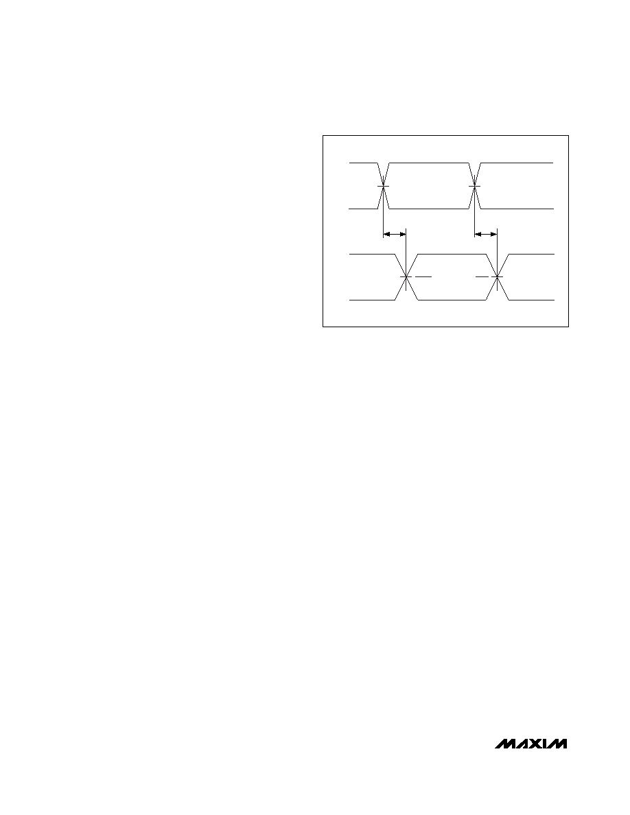
Figure 2. Timing of VP and VM to D+ and D-
VM
VP
D-
D+
tPLH_DRV
tPHL_DRV
VCRS_F , VCRS_L
VP AND VM RISE/FALL TIMES < 4ns
相關PDF資料 |
PDF描述 |
|---|---|
| MS27472P14F18P | CONN RCPT 18POS WALL MT W/PINS |
| MAX3454EETE+T | IC TXRX USB ESD-PROT 16TQFN |
| MAX3453EETE+T | IC TXRX USB ESD-PROT 16TQFN |
| MS3106F20-17S | CONN PLUG 6POS STRAIGHT W/SCKT |
| MS27473T14A18PB | CONN PLUG 18POS STRAIGHT W/PINS |
相關代理商/技術參數(shù) |
參數(shù)描述 |
|---|---|
| MAX3455EETE | 制造商:Rochester Electronics LLC 功能描述: 制造商:Maxim Integrated Products 功能描述: |
| MAX3455EEUD | 制造商:Rochester Electronics LLC 功能描述: 制造商:Maxim Integrated Products 功能描述: |
| MAX3455EEUD-T | 制造商:Maxim Integrated Products 功能描述::15KV ESD-PROTECTED USB TRANSCEIVERS - Tape and Reel |
| MAX34561EVKIT# | 功能描述:電源管理IC開發(fā)工具 12V&5V DUAL E-FUSE RoHS:否 制造商:Maxim Integrated 產品:Evaluation Kits 類型:Battery Management 工具用于評估:MAX17710GB 輸入電壓: 輸出電壓:1.8 V |
| MAX34561T+ | 功能描述:熱插拔功率分布 12V/5V Hot-Plug Switch RoHS:否 制造商:Texas Instruments 產品:Controllers & Switches 電流限制: 電源電壓-最大:7 V 電源電壓-最小:- 0.3 V 工作溫度范圍: 功率耗散: 安裝風格:SMD/SMT 封裝 / 箱體:MSOP-8 封裝:Tube |
發(fā)布緊急采購,3分鐘左右您將得到回復。