- 您現(xiàn)在的位置:買賣IC網(wǎng) > PDF目錄385527 > MAX3654 (Maxim Integrated Products, Inc.) Dual LVDS Transmitter/Receiver 16-TSSOP PDF資料下載
參數(shù)資料
| 型號(hào): | MAX3654 |
| 廠商: | Maxim Integrated Products, Inc. |
| 英文描述: | Dual LVDS Transmitter/Receiver 16-TSSOP |
| 中文描述: | 47MHz至870MHz模擬CATV互阻放大器 |
| 文件頁數(shù): | 2/8頁 |
| 文件大?。?/td> | 622K |
| 代理商: | MAX3654 |
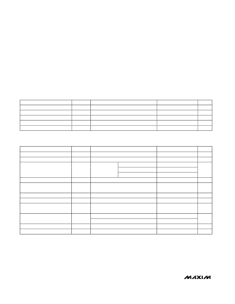
AC ELECTRICAL CHARACTERISTICS
(V
CC
= +4.75V to +5.25V, output ZL = 75
, typical values at V
CC
= +5.0V, T
A
= +25°C, unless otherwise noted.)
PARAMETER
SYM B O L
f
CONDITIONS
MIN
47
TYP
MAX
870
±0.75
63.5
54.5
45
±1.6
UNITS
MHz
dB
Operating Frequency Range
Frequency Response Flatness
47MHz to 870MHz (Notes 2, 6)
±0.3
62
53
43.5
±0.75
V
AGC
≤
0.175V
V
AGC
= 0.500V
V
AGC
= 1.400V
60.5
51.5
42
Transimpedance, Differential (Z
T
)
47MHz
dB
Gain Control Stability
V
AGC
= 0 to 1.4V, R
HYST
= open (Note 3)
Linear, 870MHz compared to 47MHz
(Notes 4, 6)
dB
Gain Tilt
3
4
5.5
dB
Output Second-Order Intercept
Output Third-Order Intercept
OIP2
OIP3
(Note 5)
(Notes 4, 5)
>47
21
dBm
dBm
18
Equivalent Input Noise Including
Photodiode
EIN
V
AGC
≤
0.175V
(Notes 4, 6)
8
pA/
√
Hz
R
HYST
= open
R
HYST
= GND
MUTE
≤
0.8V, 50MHz
47MHz to 870MHz
±0.13
±0.65
-58
13
Gain Hysteresis, Optical
dB
Differential Output Level, Mute
RF Output Return Loss
-45
dBc
dB
-S22
Note 1:
DC parameters are tested at +25°C, and guaranteed by design and characterization at -40°C and +85°C.
Note 2:
Maximum difference between frequency response at any point and a straight line connecting frequency response at
end points.
Note 3:
Gain control stability is the maximum variation in transimpedance (over process, voltage, and temperature) for any V
AGC
control voltage.
Note 4:
AC parameters guaranteed by design and characterization.
Note 5:
OIP2 and OIP3 measured using two tones at f1 = 800MHz and f2 = 850MHz, P
OUT
= -16dBm, V
AGC
= 1.4V.
Note 6:
Includes the effects of a packaged photodiode having the characteristics shown in Figure 2.
M
47MHz to 870MHz Analog CATV
Transimpedance Amplifier
2
_______________________________________________________________________________________
ABSOLUTE MAXIMUM RATINGS
Supply Voltage, VCC.............................................-0.3V to +6.0V
IN+, IN-, VAGC, OUT+, OUT-,
MUTE
, HYST.........-0.3V to +5.5V
TEST1, TEST2........................................................-0.3V to +5.5V
Output Current (OUT+, OUT-) ............................................56mA
Stresses beyond those listed under “Absolute Maximum Ratings” may cause permanent damage to the device. These are stress ratings only, and functional
operation of the device at these or any other conditions beyond those indicated in the operational sections of the specifications is not implied. Exposure to
absolute maximum rating conditions for extended periods may affect device reliability.
Continuous Power Dissipation, 16-Lead TQFN-EP Package
(T
A
= +70°C) (derate 16.9mW/°C above +70°C)....1349.1mW
Operating Temperature Range ...........................-40°C to +85°C
Storage Temperature Range.............................-55°C to +150°C
Lead Temperature (soldering,10s)..................................+300°C
DC ELECTRICAL CHARACTERISTICS
(V
CC
= +4.75V to +5.25V, typical values at V
CC
= +5.0V, T
A
= +25°C, unless otherwise noted.) (Note 1)
PARAMETER
SYM B O L
I
CC
CONDITIONS
MIN
TYP
136
50
MAX
170
200
UNITS
mA
μA
V
V
μA
Supply Current
Gain Control Input Current
Mute
Input High
Mute
Input Low
Mute
Input Current
V
AGC
= 1.4V
V
IH
V
IL
I
IL
, I
IH
2.0
0.8
30
相關(guān)PDF資料 |
PDF描述 |
|---|---|
| MAX3657 | 155Mbps Low-Noise Transimpedance Amplifier |
| MAX3657BE | 155Mbps Low-Noise Transimpedance Amplifier |
| MAX3657D | 155Mbps Low-Noise Transimpedance Amplifier |
| MAX3657E | 155Mbps Low-Noise Transimpedance Amplifier |
| MAX3657ETC | 155Mbps Low-Noise Transimpedance Amplifier |
相關(guān)代理商/技術(shù)參數(shù) |
參數(shù)描述 |
|---|---|
| MAX3654ETE+ | 功能描述:跨阻抗放大器 47-870MHz Alog CATV Transimpedance Amp RoHS:否 制造商:Texas Instruments 封裝 / 箱體:SOIC-14 帶寬:3 MHz 工作電源電壓:36 V 電源電流:5.5 mA 工作溫度范圍:- 40 C to + 85 C 封裝:Tube |
| MAX3654ETE+T | 功能描述:跨阻抗放大器 47-870MHz Alog CATV Transimpedance Amp RoHS:否 制造商:Texas Instruments 封裝 / 箱體:SOIC-14 帶寬:3 MHz 工作電源電壓:36 V 電源電流:5.5 mA 工作溫度范圍:- 40 C to + 85 C 封裝:Tube |
| MAX3654EVKIT | 功能描述:跨阻抗放大器 MAX3654 Evaluation Kit RoHS:否 制造商:Texas Instruments 封裝 / 箱體:SOIC-14 帶寬:3 MHz 工作電源電壓:36 V 電源電流:5.5 mA 工作溫度范圍:- 40 C to + 85 C 封裝:Tube |
| MAX3656E/D | 功能描述:激光驅(qū)動(dòng)器 RoHS:否 制造商:Micrel 數(shù)據(jù)速率:4.25 Gbps 工作電源電壓:3 V to 3.6 V 電源電流:80 mA 最大工作溫度:+ 85 C 封裝 / 箱體:QFN-16 封裝:Tube |
| MAX3656ETA | 制造商:Maxim Integrated Products 功能描述:- Rail/Tube |
發(fā)布緊急采購,3分鐘左右您將得到回復(fù)。