- 您現(xiàn)在的位置:買賣IC網(wǎng) > PDF目錄383418 > MAX4692EGE (MAXIM INTEGRATED PRODUCTS INC) Low-Voltage 8:1 Mux/Dual 4:1 Mux/Triple SPDT/ Quad SPDT in UCSP Package PDF資料下載
參數(shù)資料
| 型號(hào): | MAX4692EGE |
| 廠商: | MAXIM INTEGRATED PRODUCTS INC |
| 元件分類: | 運(yùn)動(dòng)控制電子 |
| 英文描述: | Low-Voltage 8:1 Mux/Dual 4:1 Mux/Triple SPDT/ Quad SPDT in UCSP Package |
| 中文描述: | 4-CHANNEL, DIFFERENTIAL MULTIPLEXER, QCC16 |
| 封裝: | 4 X 4 MM, ROHS COMPLIANT, QFN-16 |
| 文件頁(yè)數(shù): | 13/22頁(yè) |
| 文件大?。?/td> | 483K |
| 代理商: | MAX4692EGE |
第1頁(yè)第2頁(yè)第3頁(yè)第4頁(yè)第5頁(yè)第6頁(yè)第7頁(yè)第8頁(yè)第9頁(yè)第10頁(yè)第11頁(yè)第12頁(yè)當(dāng)前第13頁(yè)第14頁(yè)第15頁(yè)第16頁(yè)第17頁(yè)第18頁(yè)第19頁(yè)第20頁(yè)第21頁(yè)第22頁(yè)
M
Low-Voltage 8:1 Mux/Dual 4:1 Mux/Triple SPDT/
Quad SPDT in UCSP Package
______________________________________________________________________________________
13
During normal operation, these (and other) reverse-
biased ESD diodes leak, forming the only current
drawn from V+ or V-.
Virtually all the analog leakage current comes from the
ESD diodes. Although the ESD diodes on a given sig-
nal pin are identical, and therefore fairly well balanced,
they are reverse biased differently. Each is biased by
either V+ or V- and the analog signal. This means their
leakages will vary as the signal varies. The
difference
in
the two diode leakages to the V+ and V- pins consti-
tutes the analog signal path leakage current. All analog
leakage current flows between each pin and one of the
supply terminals, not to the other switch terminal. This
is why both sides of a given switch can show leakage
currents of either the same or opposite polarity.
V+ and GND power the internal logic and logic-level
translators, and set both the input and output logic lim-
its. The logic-level translators convert the logic levels
into switched V+ and V- signals to drive the gates of
the analog signals. This drive signal is the only connec-
tion between the logic supplies (and signals) and the
analog supplies. V+ and V- have ESD-protection
diodes on GND.
Bipolar Supplies
The MAX4691/MAX4692/MAX4693 operate with bipolar
supplies between ±2V and ±5.5V. The V+ and V- sup-
plies need not be symmetrical, but their difference can-
not exceed the absolute maximum rating of +12V.
Single Supply
These devices operate from a single supply between +2V
and +11V when V- is connected to GND. All of the bipolar
precautions must be observed. At room temperature,
they operate with a single supply at near or below +2V,
although as supply voltage decreases, switch on-resis-
tance and switching times become very high.
Always bypass supplies with a 0.1μF capacitor.
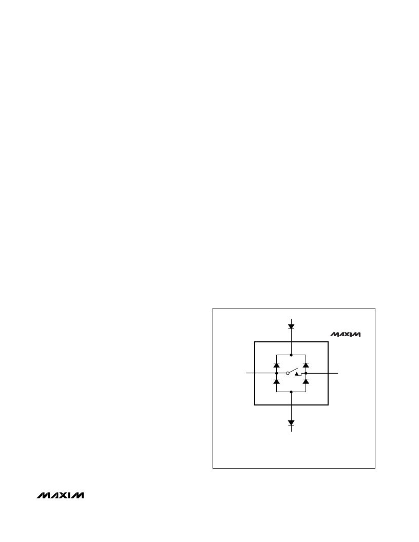
Overvoltage Protection
Proper power-supply sequencing is recommended for
all CMOS devices. Do not exceed the absolute maxi-
mum ratings, because stresses beyond the listed rat-
ings can cause permanent damage to the devices.
Always sequence V+ on first, then V-, followed by the
logic inputs and by W, X, Y, Z. If power-supply
sequencing is not possible, add two small signal
diodes (D1, D2) in series with the supply pins for over-
voltage protection (Figure 1).
Adding diodes reduces the analog signal range to one
diode drop below V+ and one diode drop above V-, but
does not affect the devices
’
low switch resistance and
low leakage characteristics. Device operation is
unchanged, and the difference between V+ and V-
should not exceed 12V. These protection diodes are
not recommended when using a single supply if signal
levels must extend to ground.
UCSP Reliability
The chip-scale package (UCSP) represents a unique
package that greatly reduces board space compared to
other packages. UCSP reliability is integrally linked to the
user
’
s assembly methods, circuit board material, and
usage environment. The user should closely review these
areas when considering a UCSP. Performance through
Operating Life Test and Moisture Resistance is equal to
conventional package technology as it is primarily deter-
mined by the wafer-fabrication process. However, this
form factor may not perform equally to a packaged prod-
uct through traditional mechanical reliability tests.
Mechanical stress performance is a greater considera-
tion for a UCSP. UCSP solder joint contact integrity
must be considered since the package is attached
through direct solder contact to the user
’
s PC board.
Testing done to characterize the UCSP reliability per-
formance shows that it is capable of performing reli-
ably through environmental stresses. Results of
environmental stress tests and additional usage data
and recommendations are detailed in the UCSP appli-
cation note, which can be found on Maxim
’
s website,
at www.maxim-ic.com.
( ) ARE FOR THE MAX4694 ONLY, REPLACE V- WITH GND.
MAX4691
MAX4692
MAX4693
MAX4694
COM
NO
V-
(GND)
V+
*INTERNAL PROTECTION DIODES
D2
D1
EXTERNAL BLOCKING DIODE
EXTERNAL BLOCKING DIODE
V- (GND )
V+
*
*
*
*
Figure 1. Overvoltage Protection
相關(guān)PDF資料 |
PDF描述 |
|---|---|
| MAX4691 | Low-Voltage 8:1 Mux/Dual 4:1 Mux/Triple SPDT/ Quad SPDT in UCSP Package |
| MAX4691EBE-T | Low-Voltage 8:1 Mux/Dual 4:1 Mux/Triple SPDT/ Quad SPDT in UCSP Package |
| MAX4692EBE-T | Low-Voltage 8:1 Mux/Dual 4:1 Mux/Triple SPDT/ Quad SPDT in UCSP Package |
| MAX4693EBE-T | Low-Voltage 8:1 Mux/Dual 4:1 Mux/Triple SPDT/ Quad SPDT in UCSP Package |
| MAX4694EBE-T | Low-Voltage 8:1 Mux/Dual 4:1 Mux/Triple SPDT/ Quad SPDT in UCSP Package |
相關(guān)代理商/技術(shù)參數(shù) |
參數(shù)描述 |
|---|---|
| MAX4692EGE+ | 制造商:Maxim Integrated Products 功能描述: 制造商:Maxim Integrated Products 功能描述:Multiplexer Switch ICs 2Ch 4:1 Mux |
| MAX4692EGE+T | 制造商:Maxim Integrated Products 功能描述:ANLG MUX DUAL 4:1 5.5V/11V 16QFN - Tape and Reel |
| MAX4692EGE-T | 功能描述:多路器開關(guān) IC RoHS:否 制造商:Texas Instruments 通道數(shù)量:1 開關(guān)數(shù)量:4 開啟電阻(最大值):7 Ohms 開啟時(shí)間(最大值): 關(guān)閉時(shí)間(最大值): 傳播延遲時(shí)間:0.25 ns 工作電源電壓:2.3 V to 3.6 V 工作電源電流: 最大工作溫度:+ 85 C 安裝風(fēng)格:SMD/SMT 封裝 / 箱體:UQFN-16 |
| MAX4692ETE+ | 功能描述:多路器開關(guān) IC 4:1 2Ch Low Voltage Analog MUX RoHS:否 制造商:Texas Instruments 通道數(shù)量:1 開關(guān)數(shù)量:4 開啟電阻(最大值):7 Ohms 開啟時(shí)間(最大值): 關(guān)閉時(shí)間(最大值): 傳播延遲時(shí)間:0.25 ns 工作電源電壓:2.3 V to 3.6 V 工作電源電流: 最大工作溫度:+ 85 C 安裝風(fēng)格:SMD/SMT 封裝 / 箱體:UQFN-16 |
| MAX4692ETE+T | 功能描述:多路器開關(guān) IC 4:1 2Ch Low Voltage Analog MUX RoHS:否 制造商:Texas Instruments 通道數(shù)量:1 開關(guān)數(shù)量:4 開啟電阻(最大值):7 Ohms 開啟時(shí)間(最大值): 關(guān)閉時(shí)間(最大值): 傳播延遲時(shí)間:0.25 ns 工作電源電壓:2.3 V to 3.6 V 工作電源電流: 最大工作溫度:+ 85 C 安裝風(fēng)格:SMD/SMT 封裝 / 箱體:UQFN-16 |
發(fā)布緊急采購(gòu),3分鐘左右您將得到回復(fù)。