- 您現(xiàn)在的位置:買賣IC網(wǎng) > PDF目錄383438 > MAX545BMJD (MAXIM INTEGRATED PRODUCTS INC) Octal 25-Ohm Buffer/Driver With 3-State Outputs 24-PDIP -40 to 85 PDF資料下載
參數(shù)資料
| 型號: | MAX545BMJD |
| 廠商: | MAXIM INTEGRATED PRODUCTS INC |
| 元件分類: | DAC |
| 英文描述: | Octal 25-Ohm Buffer/Driver With 3-State Outputs 24-PDIP -40 to 85 |
| 中文描述: | SERIAL INPUT LOADING, 1 us SETTLING TIME, 14-BIT DAC, CDIP14 |
| 封裝: | CERAMIC, DIP-14 |
| 文件頁數(shù): | 10/12頁 |
| 文件大小: | 265K |
| 代理商: | MAX545BMJD |
M
+5V, Serial-Input, Voltage-Output, 14-Bit DACs
10
______________________________________________________________________________________
amplifier’s input resistance forms a resistive divider with
the DAC output resistance, which results in a gain
error. To contribute less than 1/2LSB of gain error, the
input resistance typically must be greater than:
1
2
2
The settling time is affected by the buffer input capaci-
tance, the DAC’s output capacitance, and PC board
capacitance. The typical DAC output voltage settling
time is 1μs for a full-scale step. Settling time can be
significantly less for smaller step changes. Assuming a
single time-constant exponential settling response, a
full-scale step takes 10.4 time constants to settle to
within 1/2LSB of the final output voltage. The time con-
stant is equal to the DAC output resistance multiplied
by the total output capacitance. The DAC output
capacitance is typically 10pF. Any additional output
capacitance increases the settling time.
The external buffer amplifier’s gain-bandwidth product
is important because it increases the settling time by
adding another time constant to the output response.
The effective time constant of two cascaded systems,
each with a single time-constant response, is approxi-
mately the root square sum of the two time constants.
The DAC output’s time constant is 1μs / 10.4 = 96ns,
ignoring the effect of additional capacitance. If the time
constant of an external amplifier with 1MHz bandwidth
is 1 / 2
π
(1MHz) = 159ns, then the effective time con-
stant of the combined system is:
This suggests that the settling time to within 1/2LSB of
the final output voltage, including the external buffer
amplifier, will be approximately 10.4
·
186ns = 1.93μs.
Digital Inputs and Interface Logic
The digital interface for the 14-bit DAC is based on a
3-wire standard that is compatible with SPI, QSPI, and
MICROWIRE interfaces. The three digital inputs (
CS
,
DIN, and SCLK) load the digital input data serially into
the DAC.
LDAC
(MAX545) updates the DAC output
asynchronously.
All of the digital inputs include Schmitt-trigger buffers to
accept slow-transition interfaces. This means that opto-
couplers can interface directly to the MAX544/MAX545
without additional external logic. The digital inputs are
compatible with TTL/CMOS-logic levels.
Unipolar Configuration
Figure 2a shows the MAX544/MAX545 configured for
unipolar operation with an external op amp. The op amp
is set for unity gain, and Table 1 lists the codes for this
circuit.
Bipolar Configuration
Figure 2b shows the MAX545 configured for bipolar
operation with an external op amp. The op amp is set
for unity gain with an offset of -1/2V
REF
. Table 2 shows
the offset binary codes for this circuit.
Power-Supply Bypassing and
Ground Management
For optimum system performance, use PC boards with
separate analog and digital ground planes. Wire-wrap
boards are not recommended. Connect the two ground
planes together at the low-impedance power-supply
source. Connect DGND and AGND together at the IC.
The best ground connection can be achieved by con-
necting the DAC’s DGND and AGND pins together and
connecting that point to the system analog ground
plane. If the DAC’s DGND is connected to the system
digital ground, digital noise may get through to the
DAC’s analog portion.
Bypass V
DD
with a 0.1μF ceramic capacitor connected
between V
DD
and AGND. Mount it with short leads
close to the device. Ferrite beads can also be used to
further isolate the analog and digital power supplies.
96ns
159ns
186ns
2
2
(
)
+
(
)
6.25k
1
14
2
M
÷
=
05
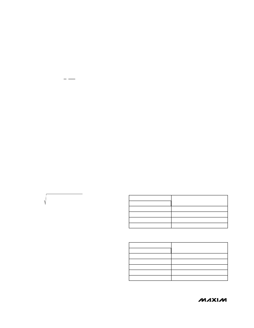
Table 1. Unipolar Code Table
Table 2. Bipolar Code Table
0V
0000 0000 0000 00(00)
V
REF
·
(1 / 16,384)
0000 0000 0000 01(00)
V
REF
·
(8192 / 16,384)=1/2V
REF
1000 0000 0000 00(00)
V
REF
·
(16,383 / 16,384)
1111 1111 1111 11(00)
ANALOG OUTPUT, V
OUT
MSB LSB
DAC LATCH CONTENTS
-V
REF
·
(8192 / 8192) = -V
REF
0000 0000 0000 00(00)
-V
REF
·
(1 / 8192)
0111 1111 1111 11(00)
0V
1000 0000 0000 00(00)
+V
REF
·
(1 / 8192)
1000 0000 0000 01(00)
+V
REF
·
(8191 / 8192)
1111 1111 1111 11(00)
ANALOG OUTPUT, V
OUT
MSB LSB
DAC LATCH CONTENTS
( ) = Sub-bits
相關(guān)PDF資料 |
PDF描述 |
|---|---|
| MAX545BCPD | +5V, Serial-Input, Voltage-Output, 14-Bit DACs |
| MAX544 | +5V, Serial-Input, Voltage-Output, 14-Bit DACs |
| MAX5461EXT | 32-Tap. Nonvolatile. Linear-Taper Digital Potentiometers in SOT23 |
| MAX5461 | TOOL |
| MAX5462 | TOOL |
相關(guān)代理商/技術(shù)參數(shù) |
參數(shù)描述 |
|---|---|
| MAX5460EXK | 制造商:Maxim Integrated Products 功能描述:- Rail/Tube |
| MAX5460EXK+ | 制造商:Maxim Integrated Products 功能描述:DGTL POTENTIOMETER 32POS 100KOHM SGL 5PIN SC-70 - Rail/Tube |
| MAX5460EXK+T | 功能描述:數(shù)字電位計(jì) IC 32-Tap FleaPoT 2Wire RoHS:否 制造商:Maxim Integrated 電阻:200 Ohms 溫度系數(shù):35 PPM / C 容差:25 % POT 數(shù)量:Dual 每 POT 分接頭:256 弧刷存儲器:Volatile 緩沖刷: 數(shù)字接口:Serial (3-Wire, SPI) 描述/功能:Dual Volatile Low Voltage Linear Taper Digital Potentiometer 工作電源電壓:1.7 V to 5.5 V 電源電流:27 uA 最大工作溫度:+ 125 C 安裝風(fēng)格:SMD/SMT 封裝 / 箱體:TQFN-16 封裝:Reel |
| MAX5460EXK-T | 功能描述:數(shù)字電位計(jì) IC RoHS:否 制造商:Maxim Integrated 電阻:200 Ohms 溫度系數(shù):35 PPM / C 容差:25 % POT 數(shù)量:Dual 每 POT 分接頭:256 弧刷存儲器:Volatile 緩沖刷: 數(shù)字接口:Serial (3-Wire, SPI) 描述/功能:Dual Volatile Low Voltage Linear Taper Digital Potentiometer 工作電源電壓:1.7 V to 5.5 V 電源電流:27 uA 最大工作溫度:+ 125 C 安裝風(fēng)格:SMD/SMT 封裝 / 箱體:TQFN-16 封裝:Reel |
| MAX5461EXT | 制造商:Maxim Integrated Products 功能描述:32-TAP FLEAPOT 2-WIRE DIGITAL POTEN - Cut Tape Product |
發(fā)布緊急采購,3分鐘左右您將得到回復(fù)。