- 您現(xiàn)在的位置:買(mǎi)賣(mài)IC網(wǎng) > PDF目錄385542 > MAX6666 (Maxim Integrated Products, Inc.) 3-Line To 8-Line Decoder/Demultiplexer 20-LCCC -55 to 125 PDF資料下載
參數(shù)資料
| 型號(hào): | MAX6666 |
| 廠商: | Maxim Integrated Products, Inc. |
| 英文描述: | 3-Line To 8-Line Decoder/Demultiplexer 20-LCCC -55 to 125 |
| 中文描述: | 高精度PWM輸出溫度傳感器 |
| 文件頁(yè)數(shù): | 2/8頁(yè) |
| 文件大?。?/td> | 268K |
| 代理商: | MAX6666 |
M
High-Accuracy PWM Output Temperature
Sensors
2
_______________________________________________________________________________________
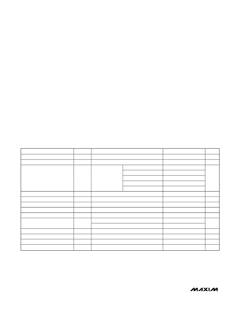
ABSOLUTE MAXIMUM RATINGS
(Voltages Referenced to GND)
V
CC
........................................................................-0.3V to +6.0V
D
OUT
MAX6666................................................-0.3V to (V
CC
+ 0.3V)
MAX6667..........................................................-0.3V to + 6.0V
D
OUT
Current ......................................................-1mA to +50mA
Continuous Current into Any Other Terminal....................±20mA
ELECTRICAL CHARACTERISTICS
(V
CC
= +3.0V to +5.5V, T
A
= -40
°
C to +125
°
C, unless otherwise noted. Typical values are at V
CC
= +3.3V, T
A
= +25
°
C.)
Stresses beyond those listed under “Absolute Maximum Ratings” may cause permanent damage to the device. These are stress ratings only, and functional
operation of the device at these or any other conditions beyond those indicated in the operational sections of the specifications is not implied. Exposure to
absolute maximum rating conditions for extended periods may affect device reliability.
Continuous Power Dissipation (T
A
= +70
°
C)
6-Pin SOT23 (derate 8.7mW/
°
C above +70
°
C).........695.7mW
8-Pin μMAX (derate 4.1mW/
°
C above +70
°
C).............330mW
8-Pin SO (derate 5.88mW/
°
C above +70
°
C)................471mW
Operating Temperature Range .........................-40
°
C to +150
°
C
Storage Temperature Range.............................-65
°
C to +150
°
C
Junction Temperature......................................................+150
°
C
Lead Temperature (soldering,10s).....................................+150
°
PARAMETER
SYMBOL
V
CC
I
CC
CONDITIONS
MIN
3.0
TYP
MAX
5.5
500
+1
+2.5
+3.8
+4.8
+6
UNITS
V
μA
Supply Voltage Range
Supply Current
V
CC
= +3.0V to +5.5V
200
T
A
= +30
°
C
T
A
= +10
°
C to +50
°
C
T
A
= 0
°
C to +100
°
C
T
A
= -25
°
C to +125
°
C
T
A
= -40
°
C, V
CC
= +3.3V
-1
-2.5
-3.8
-4.8
-6
Temperature Error
V
CC
= +3.3V
°
C
Nominal t
1
Pulse Width
MAX6666 Output High Voltage
MAX6666 Output Low Voltage
MAX6666 Fall Time
MAX6666 Rise Time
10
ms
V
V
ns
ns
I
OH
= 800μA
I
OL
= 800μA
C
L
= 100pF, R
L
=
∞
C
L
= 100pF, R
L
=
∞
I
SINK
= 1.6mA
I
SINK
= 5.0mA
C
L
= 100pF, R
L
= 10k
C
L
= 0
V
C C
- 0.4
0.4
80
80
0.4
1.2
MAX6667 Output Low Voltage
V
MAX6667 Fall Time
MAX6667 Output Capacitance
MAX6667 Output Leakage
Power-Supply Rejection Ratio
40
15
<0.1
0.3
ns
pF
μA
°
C/V
PSRR
V
CC
= +3.0V to +5.5V
1.0
相關(guān)PDF資料 |
PDF描述 |
|---|---|
| MAX6666ASA | 3-Line To 8-Line Decoder/Demultiplexer 16-CDIP -55 to 125 |
| MAX6666AUA | 3-Line To 8-Line Decoder/Demultiplexer 16-CFP -55 to 125 |
| MAX6667ASA | High-Accuracy PWM Output Temperature Sensors |
| MAX6667AUA | High-Accuracy PWM Output Temperature Sensors |
| MAX667 | +5V/Programmable Low-Dropout Voltage Regulator(5V/可調(diào),低輸出步降線(xiàn)性穩(wěn)壓器) |
相關(guān)代理商/技術(shù)參數(shù) |
參數(shù)描述 |
|---|---|
| MAX6666ASA | 制造商:Maxim Integrated Products 功能描述:HIGH-ACCURACY PWM OUTPUT TEMPERATURE SENSORS - Bulk |
| MAX6666ATT+T | 制造商:Maxim Integrated Products 功能描述:HIGH-ACCURACY PWM OUTPUT TEMPERATUR - Tape and Reel |
| MAX6666AUA | 制造商:Maxim Integrated Products 功能描述:HIGH-ACCURACY PWM OUTPUT TEMPERATURE SENSORS - Bulk |
| MAX6666AUA+ | 制造商:Maxim Integrated Products 功能描述:TEMP SENSOR DGTL 1-WIRE 8PIN UMAX - Rail/Tube |
| MAX6666AUA+T | 制造商:Maxim Integrated Products 功能描述:TEMP SENSOR DGTL SERL (1-WIRE) 8PIN UMAX - Tape and Reel |
發(fā)布緊急采購(gòu),3分鐘左右您將得到回復(fù)。