- 您現在的位置:買賣IC網 > PDF目錄69018 > MAX6917EO30 (MAXIM INTEGRATED PRODUCTS INC) REAL TIME CLOCK, PDSO20 PDF資料下載
參數資料
| 型號: | MAX6917EO30 |
| 廠商: | MAXIM INTEGRATED PRODUCTS INC |
| 元件分類: | 時鐘/數據恢復及定時提取 |
| 英文描述: | REAL TIME CLOCK, PDSO20 |
| 封裝: | 0.150 INCH, 0.025 INCH PITCH, MO-137AD, QSOP-20 |
| 文件頁數: | 5/31頁 |
| 文件大小: | 349K |
| 代理商: | MAX6917EO30 |
第1頁第2頁第3頁第4頁當前第5頁第6頁第7頁第8頁第9頁第10頁第11頁第12頁第13頁第14頁第15頁第16頁第17頁第18頁第19頁第20頁第21頁第22頁第23頁第24頁第25頁第26頁第27頁第28頁第29頁第30頁第31頁

MAX6917
I2C-Compatible RTC with Microprocessor
Supervisor, Alarm, and NV RAM Controller
______________________________________________________________________________________
13
To maximize battery life and prevent erroneous data
from being entered into the MAX6917, the serial bus
interface is disabled when VCC is below VRST. If the
SDA or SCL serial interface lines are held low for longer
than 1s to 2s, the serial bus interface resets and awaits
for a new START condition (see the START and STOP
Conditions section).
I2C System Configuration
A device on the I2C-compatible bus that generates a
message is called a transmitter and a device that
receives the message is called a receiver. The device
that controls the message is the master and the
devices that are controlled by the master are called
slaves (Figure 3). The word message refers to data in
the form of three 8-bit bytes for a single read or write.
The first byte is the slave ID byte, the second byte is
the address/command byte, and the third is the data.
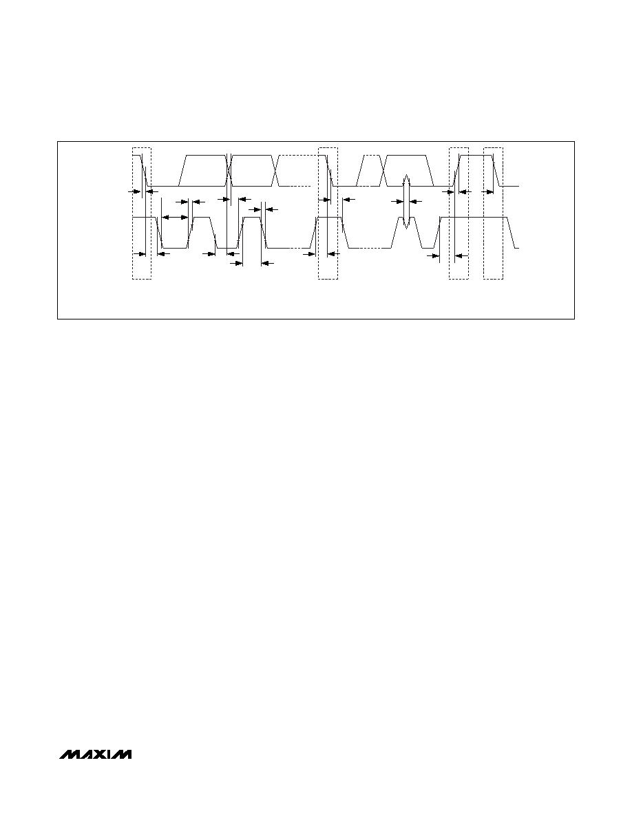
START and STOP Conditions
Data transfer can only be initiated when the bus is not
busy (both SDA and SCL are high). A high-to-low tran-
sition of SDA while SCL is high defines a START (S)
condition; low-to-high transition of SDA while SCL is
high defines a STOP (P) condition (Figures 2, 4). Any
time a START condition occurs, the slave ID must follow
immediately, regardless of completion of a previous
data transfer.
Bit Transfer
After the START condition occurs, 1 bit of data is trans-
ferred for each clock pulse. The data on SDA must
remain stable during the high portion of the clock pulse
as changes in data during this time are interpreted as a
control signal (Figure 5).
Acknowledge
The acknowledge bit is a clocked 9th bit that the recipi-
ent uses to handshake receipt of each byte of data
(Figure 6). Thus, each byte transferred effectively
requires 9 bits. The master generates the 9th clock
pulse, and the recipient pulls down SDA during the
acknowledge clock pulse, such that the SDA line is sta-
ble low during the high portion of the clock pulse. A
master receiver must signal an end of data to the trans-
mitter by not generating an acknowledge on the last
byte that has been clocked out of the slave. In this
case, the transmitter must leave the SDA high to enable
the master to generate a STOP condition. If a STOP
condition is received before the current byte of data
transfer is completed in burst mode, the last incomplete
byte is ignored if it is a burst transaction to RAM or the
whole burst transaction is ignored if it is a burst trans-
action to the timekeeping registers. There is no limit to
the number of bytes that can be transmitted between a
START and a STOP condition.
Slave Address
Before any data is transmitted on the I2C-bus-compati-
ble serial interface, the device that is expected to
respond must be addressed first. The first byte sent
after the START (S) condition is the address byte or 7-
bit slave ID. The MAX6917 acts as a slave trans-
mitter/receiver. Therefore, SCL is only an input clock
signal and SDA is a bidirectional data line. The slave
address for the MAX6917 is shown in Figure 7.
SDA
SCL
tF
tR
tLOW
tSU:DAT
tF
tHD:STA
tHD:DAT
tHIGH
tSU:STA
tHD:STA
tSP
tSU:STO
tR
tBUFF
P
S
Sr
S = START CONDITION
P = STOP CONDITION
Sr = REPEATED START CONDITION
Figure 2. I2C Communication Timing Diagram
相關PDF資料 |
PDF描述 |
|---|---|
| MAX6917EO33 | REAL TIME CLOCK, PDSO20 |
| MAX8893AEWV+ | SPECIALTY MICROPROCESSOR CIRCUIT, PBGA30 |
| MAX8893BEWV+ | SPECIALTY MICROPROCESSOR CIRCUIT, PBGA30 |
| MAX8893CEWV+ | SPECIALTY MICROPROCESSOR CIRCUIT, PBGA30 |
| MAX9485ETP+ | 73.728 MHz, OTHER CLOCK GENERATOR, QCC20 |
相關代理商/技術參數 |
參數描述 |
|---|---|
| MAX6917EO30+ | 功能描述:實時時鐘 Integrated Circuits (ICs) RoHS:否 制造商:Microchip Technology 功能:Clock, Calendar. Alarm RTC 總線接口:I2C 日期格式:DW:DM:M:Y 時間格式:HH:MM:SS RTC 存儲容量:64 B 電源電壓-最大:5.5 V 電源電壓-最小:1.8 V 最大工作溫度:+ 85 C 最小工作溫度: 安裝風格:Through Hole 封裝 / 箱體:PDIP-8 封裝:Tube |
| MAX6917EO30+T | 功能描述:實時時鐘 Integrated Circuits (ICs) RoHS:否 制造商:Microchip Technology 功能:Clock, Calendar. Alarm RTC 總線接口:I2C 日期格式:DW:DM:M:Y 時間格式:HH:MM:SS RTC 存儲容量:64 B 電源電壓-最大:5.5 V 電源電壓-最小:1.8 V 最大工作溫度:+ 85 C 最小工作溫度: 安裝風格:Through Hole 封裝 / 箱體:PDIP-8 封裝:Tube |
| MAX6917EO33+ | 功能描述:實時時鐘 Integrated Circuits (ICs) RoHS:否 制造商:Microchip Technology 功能:Clock, Calendar. Alarm RTC 總線接口:I2C 日期格式:DW:DM:M:Y 時間格式:HH:MM:SS RTC 存儲容量:64 B 電源電壓-最大:5.5 V 電源電壓-最小:1.8 V 最大工作溫度:+ 85 C 最小工作溫度: 安裝風格:Through Hole 封裝 / 箱體:PDIP-8 封裝:Tube |
| MAX6917EO33+T | 功能描述:實時時鐘 Integrated Circuits (ICs) RoHS:否 制造商:Microchip Technology 功能:Clock, Calendar. Alarm RTC 總線接口:I2C 日期格式:DW:DM:M:Y 時間格式:HH:MM:SS RTC 存儲容量:64 B 電源電壓-最大:5.5 V 電源電壓-最小:1.8 V 最大工作溫度:+ 85 C 最小工作溫度: 安裝風格:Through Hole 封裝 / 箱體:PDIP-8 封裝:Tube |
| MAX6917EO50 | 功能描述:實時時鐘 RoHS:否 制造商:Microchip Technology 功能:Clock, Calendar. Alarm RTC 總線接口:I2C 日期格式:DW:DM:M:Y 時間格式:HH:MM:SS RTC 存儲容量:64 B 電源電壓-最大:5.5 V 電源電壓-最小:1.8 V 最大工作溫度:+ 85 C 最小工作溫度: 安裝風格:Through Hole 封裝 / 箱體:PDIP-8 封裝:Tube |
發(fā)布緊急采購,3分鐘左右您將得到回復。