- 您現(xiàn)在的位置:買賣IC網(wǎng) > PDF目錄383540 > MAX9153EUI (MAXIM INTEGRATED PRODUCTS INC) Low-Jitter, 800Mbps, 10-Port LVDS Repeaters with 100 зDrive PDF資料下載
參數(shù)資料
| 型號: | MAX9153EUI |
| 廠商: | MAXIM INTEGRATED PRODUCTS INC |
| 元件分類: | 通用總線功能 |
| 英文描述: | Low-Jitter, 800Mbps, 10-Port LVDS Repeaters with 100 зDrive |
| 中文描述: | LINE TRANSCEIVER, PDSO28 |
| 封裝: | 4.40 MM, TSSOP-28 |
| 文件頁數(shù): | 2/11頁 |
| 文件大?。?/td> | 208K |
| 代理商: | MAX9153EUI |
M
Low-Jitter, 800Mbps, 10-Port LVDS
Repeaters with 100
Drive
2
_______________________________________________________________________________________
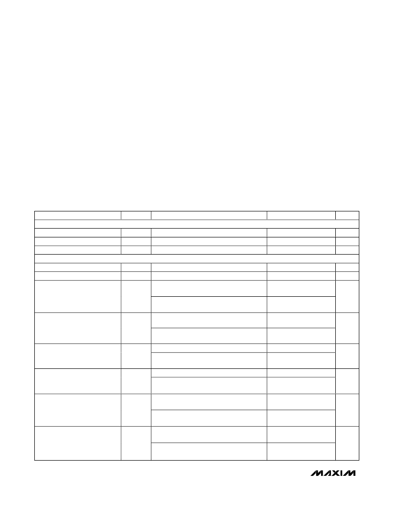
ABSOLUTE MAXIMUM RATINGS
V
CC
to GND...........................................................-0.3V to +4.0V
RIN+, RIN- to GND................................................-0.3V to +4.0V
PWRDN
to GND..........................................-0.3V to (V
CC
+ 0.3V)
DO_+, DO_- to GND..............................................-0.3V to +4.0V
Short-Circuit Duration (DO_+, DO_-) .........................Continuous
Continuous Power Dissipation (T
A
= +70
°
C)
28-Pin TSSOP (derate 12.8mW/
°
C above +70
°
C) .....1026mW
DC ELECTRICAL CHARACTERISTICS
(V
CC
= +3.0V to +3.6V, R
L
= 100
±1%, differential input voltage |V
ID
| = 0.05V to 1.2V, MAX9153 LVDS input common-mode voltage
V
CM
= |V
ID
/2| to 2.4V - |V
ID
/2|, MAX9154 LVPECL input voltage range = 0 to V
CC
,
PWRDN
= high, T
A
= -40
°
C to +85
°
C, unless other-
wise noted. Typical values are at V
CC
= +3.3V, |V
ID
| = 0.2V, V
CM
= 1.2V, T
A
= +25
°
C.) (Notes 1 and 2)
Stresses beyond those listed under “Absolute Maximum Ratings” may cause permanent damage to the device. These are stress ratings only, and functional
operation of the device at these or any other conditions beyond those indicated in the operational sections of the specifications is not implied. Exposure to
absolute maximum rating conditions for extended periods may affect device reliability.
Storage Temperature.........................................-65
°
C to +150
°
C
Maximum Junction Temperature .....................................+150
°
C
Operating Temperature Range ...........................-40
°
C to +85
°
C
ESD Protection
Human Body Model (RIN+, RIN-, DO_+, DO_-) ..............±8kV
Lead Temperature (soldering, 10s).................................+300
°
C
PARAMETER
SYMBOL
CONDITIONS
MIN
TYP
MAX
UNITS
CONTROL INPUT (
PWRDN
)
Input High Voltage
Input Low Voltage
Input Current
DIFFERENTIAL INPUT (RIN+, RIN-)
Differential Input High Threshold
Differential Input Low Threshold
V
IH
V
IL
I
IN
2.0
GND
-20
V
CC
0.8
20
V
V
μA
PWRDN
= high or low
V
TH
V
TL
-3
-3
50
mV
mV
-50
0.05V
≤
| V
ID
|
≤
0.6V,
PWRDN
= high or low
(Figure 1)
0.6V < | V
ID
|
≤
1.2V,
PWRDN
= high or low
(Figure 1)
0.05V
≤
| V
ID
|
≤
0.6V, V
CC
= 0 or open,
PWRDN
= 0 or open (Figure 1)
0.6V < | V
ID
|
≤
1.2V, V
CC
= 0 or open,
PWRDN
= 0 or open (Figure 1)
PWRDN
= high or low (Figure 1)
V
CC
= 0 or open,
PWRDN
= 0 or open
(Figure 1)
PWRDN
= high or low (Figure 1)
V
CC
= 0 or open,
PWRDN
= 0 or
open(Figure 1)
-15
-3
15
Input Current (MAX9153)
I
RIN+
,
I
RIN-
-20
-4
20
μA
-15
3
15
Power-Off Input Current
(MAX9153)
I
RIN+ (OFF)
,
I
RIN- (OFF)
-20
4
20
μA
103
Input Resistor 1 (MAX9153)
R
IN1
103
k
154
Input Resistor 2 (MAX9153)
R
IN2
154
k
V
RIN+
= 3.6V, V
RIN-
= 3.6V or 0,
PWRDN
=
high or low (Figure 2)
V
RIN+
= 0, V
RIN-
= 3.6V or 0,
PWRDN
=
high or low (Figure 2)
-10
3
10
Input Current (MAX9154)
I
RIN+
,
I
RIN-
-10
±3
10
μA
V
RIN+
= 3.6V, V
RIN-
= 0, V
CC
= 0 or open,
PWRDN
= 0 or open (Figure 2)
-10
3
10
Power-Off Input Current
(MAX9154)
I
RIN+ (OFF)
,
I
RIN- (OFF)
V
RIN+
= 0, V
RIN-
= 3.6V, V
CC
= 0 or open,
PWRDN
= 0 or open (Figure 2)
-10
3
10
μA
相關(guān)PDF資料 |
PDF描述 |
|---|---|
| MAX9153 | Low-Jitter, 800Mbps, 10-Port LVDS Repeaters with 100 зDrive |
| MAX9154EUI | Low-Jitter, 800Mbps, 10-Port LVDS Repeaters with 100 зDrive |
| MAX9155EXT-T | Low-Jitter, Low-Noise LVDS Repeater in an SC70 Package |
| MAX9155 | Low-Jitter, Low-Noise LVDS Repeater in an SC70 Package |
| MAX9156EXT-T | Low-Jitter, Low-Noise LVPECL-to-LVDS Level Translator in an SC70 Package |
相關(guān)代理商/技術(shù)參數(shù) |
參數(shù)描述 |
|---|---|
| MAX9153EUI+ | 功能描述:LVDS 接口集成電路 800Mbps 10-Port LVDS Repeater RoHS:否 制造商:Texas Instruments 激勵器數(shù)量:4 接收機數(shù)量:4 數(shù)據(jù)速率:155.5 Mbps 工作電源電壓:5 V 最大功率耗散:1025 mW 最大工作溫度:+ 85 C 封裝 / 箱體:SOIC-16 Narrow 封裝:Reel |
| MAX9153EUI+T | 功能描述:LVDS 接口集成電路 800Mbps 10-Port LVDS Repeater RoHS:否 制造商:Texas Instruments 激勵器數(shù)量:4 接收機數(shù)量:4 數(shù)據(jù)速率:155.5 Mbps 工作電源電壓:5 V 最大功率耗散:1025 mW 最大工作溫度:+ 85 C 封裝 / 箱體:SOIC-16 Narrow 封裝:Reel |
| MAX9153EUI-T | 制造商:Maxim Integrated Products 功能描述:LOW-JITTER, 800MBPS, 10-PORT LVDS REPEATERS W - Tape and Reel |
| MAX9154 | 制造商:MAXIM 制造商全稱:Maxim Integrated Products 功能描述:Low-Jitter.800Mbps.10-Port LVDS Repeaters with 100<img src=http://dbserv.maxim-ic.com/images/ohm.gif width=12 height=9 Drive |
| MAX9154EUI | 制造商:Maxim Integrated Products 功能描述:LOW-JITTER, 800MBPS, 10-PORT LVDS REPEATERS W - Rail/Tube |
發(fā)布緊急采購,3分鐘左右您將得到回復(fù)。