- 您現(xiàn)在的位置:買賣IC網(wǎng) > PDF目錄11116 > MAX9176EUB+ (Maxim Integrated Products)IC MULTIPLEXER 2:1 670MHZ 10UMAX PDF資料下載
參數(shù)資料
| 型號(hào): | MAX9176EUB+ |
| 廠商: | Maxim Integrated Products |
| 文件頁數(shù): | 9/14頁 |
| 文件大小: | 0K |
| 描述: | IC MULTIPLEXER 2:1 670MHZ 10UMAX |
| 標(biāo)準(zhǔn)包裝: | 50 |
| 系列: | * |
MAX9176/MAX9177
670MHz LVDS-to-LVDS and
Anything-to-LVDS 2:1 Multiplexers
4
_______________________________________________________________________________________
Note 1: Current into a pin is defined as positive. Current out of a pin is defined as negative. All voltages are referenced to ground
except VTH, VTL, VID, VOD, and
VOD.
Note 2: Maximum and minimum limits over temperature are guaranteed by design and characterization. Devices are 100% tested
at TA = +25°C.
Note 3: Tolerance on all external resistors (including figures) is ±1%.
Note 4: Guaranteed by design and characterization.
Note 5: AC parameters are guaranteed by design and characterization and not production tested. Limits are set at
±6 sigma.
Note 6: CL includes scope probe and test jig capacitance.
Note 7: Pulse-generator output for differential inputs IN_+, IN_- (unless otherwise noted): f = 670MHz, 50% duty cycle, RO = 50
,
tR = 500ps, and tF = 500ps (0% to 100%). Pulse-generator output for single-ended inputs PD, SEL: tR = tF = 1.5ns (0.2VCC
to 0.8VCC), 50% duty cycle, VOH = VCC + 1.0V settling to VCC, VOL = -1.0V settling to zero.
Note 8: Pulse-generator output for tDJ: VOD = 0.15V, VOS = 1.25V, bit rate = 800Mbps, 223 - 1 PRBS, RO = 50
, tR = 500ps, and tF
= 500ps (0% to 100%).
Note 9: tSKPP1 is the magnitude of the difference of any differential propagation delays between devices operating under identical
conditions.
Note 10: tSKPP2 is the magnitude of the difference of any differential propagation delays between devices operating over rated
conditions.
Note 11: Meets all AC specifications.
Note 12: Input jitter subtracted from output jitter.
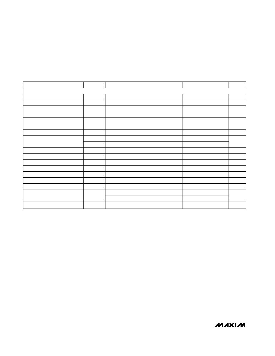
AC ELECTRICAL CHARACTERISTICS
(VCC = 3.0V to 3.6V, RL = 100
, CL = 5pF, differential input voltage |VID| = 0.15V to 1.2V, MAX9176 input common-mode voltage
VCM = |VID/2| to 2.4V - |VID/2|, MAX9177 input common-mode voltage VCM = |VID/2| to VCC - |VID/2|, TA = -40°C to +85°C, unless oth-
erwise noted. Typical values are at VCC = 3.3V,
|VID| = 0.2V, VCM = 1.25V, TA = +25°C.) (Notes 5, 6, 7)
PARAMETER
SYMBOL
CONDITIONS
MIN
TYP
MAX
UNITS
DIFFERENTIAL INPUTS (IN_+, IN_-)
High-to-Low Propagation Delay
tPHL
Figures 4, 5
1.33
2.46
3.23
ns
Low-to-High Propagation Delay
tPLH
Figures 4, 5
1.33
2.49
3.31
ns
Added Deterministic Jitter
tDJ
Figures 4, 5 (Notes 8, 12)
68
80
ps(P-P)
Added Random Jitter
tRJ
Figures 4, 5 (Note 12)
0.7
1.0
ps(RMS)
Pulse Skew
tPLH - tPHL
tSKP
Figures 4, 5
27
142
ps
tSKPP1
Figures 4, 5 (Note 9)
0.4
1.3
Part-to-Part Skew
tSKPP2
Figures 4, 5 (Note 10)
2.0
ns
Rise Time
tR
Figures 4, 5
217
320
383
ps
Fall Time
tF
Figures 4, 5
157
340
360
ps
Select to Out Delay
tPSO
Figure 6
2.0
2.7
ns
Power-Down Time
tPD
Figures 7, 8
6.0
ns
Power-Up Time
tPU
Figures 7, 8
35
s
Maximum Data Rate
DRMAX
Figures 4, 5,
VOD ≥ 250mV (Note 11)
800
Mbps
Maximum Switching Frequency
fMAX
Figures 4, 5,
VOD ≥ 250mV (Note 11)
670
MHz
fIN = 670MHz
38
58
Switching Supply Current
ICCSW
fIN = 155MHz
26
47
mA
PRBS Supply Current
ICCPR
DR = 800Mbps, 2
23 - 1 PRBS input
27
49
mA
相關(guān)PDF資料 |
PDF描述 |
|---|---|
| MAX334EWE+T | IC SWITCH QUAD SPST 16SOIC |
| DG411CUE+ | IC SWITCH QUAD SPST 16TSSOP |
| DG390ACWE+T | IC SWITCH DUAL SPDT 16SOIC |
| VI-2WJ-IW | CONVERTER MOD DC/DC 36V 100W |
| VI-2WH-IY-F4 | CONVERTER MOD DC/DC 52V 50W |
相關(guān)代理商/技術(shù)參數(shù) |
參數(shù)描述 |
|---|---|
| MAX9176EUB+ | 功能描述:LVDS 接口集成電路 670MHz LVDS->LVDS & X->LVDS 2:1 MUX RoHS:否 制造商:Texas Instruments 激勵(lì)器數(shù)量:4 接收機(jī)數(shù)量:4 數(shù)據(jù)速率:155.5 Mbps 工作電源電壓:5 V 最大功率耗散:1025 mW 最大工作溫度:+ 85 C 封裝 / 箱體:SOIC-16 Narrow 封裝:Reel |
| MAX9176EUB+T | 功能描述:LVDS 接口集成電路 670MHz LVDS->LVDS & X->LVDS 2:1 MUX RoHS:否 制造商:Texas Instruments 激勵(lì)器數(shù)量:4 接收機(jī)數(shù)量:4 數(shù)據(jù)速率:155.5 Mbps 工作電源電壓:5 V 最大功率耗散:1025 mW 最大工作溫度:+ 85 C 封裝 / 箱體:SOIC-16 Narrow 封裝:Reel |
| MAX9177 | 制造商:MAXIM 制造商全稱:Maxim Integrated Products 功能描述:670MHz LVDS-to-LVDS and Anything-to-LVDS 2:1 Multiplexers |
| MAX9177ETB | 制造商:MAXIM 制造商全稱:Maxim Integrated Products 功能描述:670MHz LVDS-to-LVDS and Anything-to-LVDS 2:1 Multiplexers |
| MAX9177EUB | 制造商:Maxim Integrated Products 功能描述:670MHZ LVDS-TO-LVDS AND ANYTHING"-TO-LVDS2:" - Rail/Tube |
發(fā)布緊急采購,3分鐘左右您將得到回復(fù)。