- 您現(xiàn)在的位置:買(mǎi)賣(mài)IC網(wǎng) > PDF目錄377879 > MB15F74UVPVB (FUJITSU LTD) Dual Serial Input PLL Frequency Synthesizer PDF資料下載
參數(shù)資料
| 型號(hào): | MB15F74UVPVB |
| 廠商: | FUJITSU LTD |
| 元件分類(lèi): | XO, clock |
| 英文描述: | Dual Serial Input PLL Frequency Synthesizer |
| 中文描述: | PLL FREQUENCY SYNTHESIZER, 4000 MHz, PBCC18 |
| 封裝: | PLASTIC, BCC-18 |
| 文件頁(yè)數(shù): | 3/25頁(yè) |
| 文件大小: | 131K |
| 代理商: | MB15F74UVPVB |
第1頁(yè)第2頁(yè)當(dāng)前第3頁(yè)第4頁(yè)第5頁(yè)第6頁(yè)第7頁(yè)第8頁(yè)第9頁(yè)第10頁(yè)第11頁(yè)第12頁(yè)第13頁(yè)第14頁(yè)第15頁(yè)第16頁(yè)第17頁(yè)第18頁(yè)第19頁(yè)第20頁(yè)第21頁(yè)第22頁(yè)第23頁(yè)第24頁(yè)第25頁(yè)
MB15F74UV
3
I
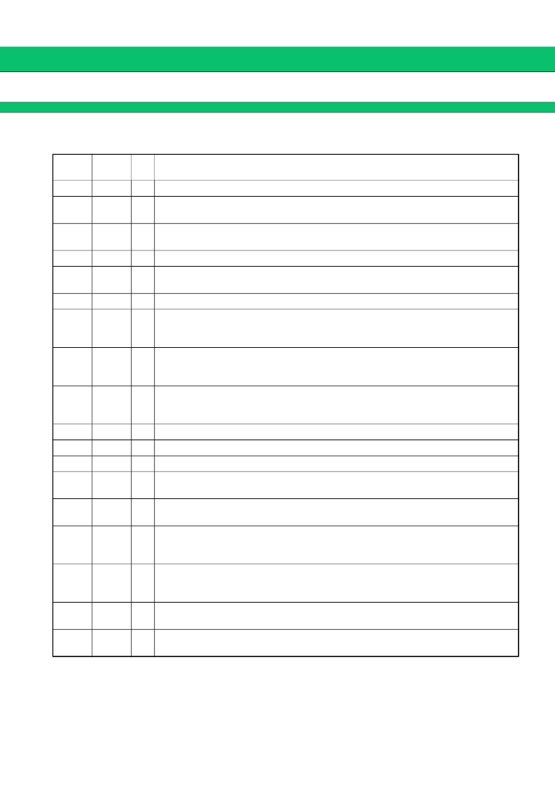
PIN DESCRIPTION
Pin no.
Pin
name
I/O
Descriptions
1
GND
Ground pin for OSC input buffer and the shift register circuit.
2
fin
IF
I
Prescaler input pin for the IF-PLL.
Connection to an external VCO should be AC coupling.
3
Xfin
IF
I
Prescaler complimentary input for the IF-PLL section.
This pin should be grounded via a capacitor.
4
GND
IF
Ground pin for the IF-PLL section.
5
V
CCIF
Power supply voltage input pin for the IF-PLL section, the shift register and the oscillator
input buffer.
6
Do
IF
O
Charge pump output for the IF-PLL section.
7
PS
IF
I
Power saving mode control pin for the IF-PLL section. This pin must be set at “L” when
the power supply is started up. (Open is prohibited.)
PS
IF
=
“H” ; Normal mode/PS
IF
=
“L” ; Power saving mode
Lock detect signal output (LD) /phase comparator monitoring output (fout) pin. The out-
put signal is selected by LDS bit in a serial data.
LDS bit
=
“H” ; outputs fout signal/LDS bit
=
“L” ; outputs LD signal
Power saving mode control for the RF-PLL section. This pin must be set at “L” when the
power supply is started up. (Open is prohibited. )
PS
RF
=
“H” ; Normal mode/PS
RF
=
“L” ; Power saving mode
Charge pump output for the RF-PLL section.
8
LD/fout
O
9
PS
RF
I
10
Do
RF
O
11
V
CCRF
Power supply voltage input pin for the RF-PLL section.
12
GND
RF
Ground pin for the RF-PLL section
13
Xfin
RF
I
Prescaler complimentary input pin for the RF-PLL section.
This pin should be grounded via a capacitor.
14
fin
RF
I
Prescaler input pin for the RF-PLL.
Connection to an external VCO should be via AC coupling.
15
LE
I
Load enable signal input pin (with the schmitt trigger circuit)
When LE is set “H”, data in the shift register is transferred to the corresponding latch ac-
cording to the control bit in a serial data.
16
Data
I
Serial data input pin (with the schmitt trigger circuit)
Data is transferred to the corresponding latch (IF-ref. counter, IF-prog. counter,
RF-ref. counter, RF-prog. counter) according to the control bit in a serial data.
17
Clock
I
Clock input pin for the 23-bit shift register (with the schmitt trigger circuit)
One bit data is shifted into the shift register on a rising edge of the clock.
18
OSC
IN
I
The programmable reference divider input pin. TCXO should be connected with an AC
coupling capacitor.
相關(guān)PDF資料 |
PDF描述 |
|---|---|
| MB15F76ULPVA | Dual Serial Input PLL Frequency Synthesizer |
| MB15F76UV | ASSP Dual Serial Input PLL Frequency Synthesizer(Small Package) |
| MB15F78SP | Dual Serial Input PLL Frequency Synthesizer |
| MB15F78SPPFT | Dual Serial Input PLL Frequency Synthesizer |
| MB15F78SPPV | Dual Serial Input PLL Frequency Synthesizer |
相關(guān)代理商/技術(shù)參數(shù) |
參數(shù)描述 |
|---|---|
| MB15F76UL | 制造商:FUJITSU 制造商全稱(chēng):Fujitsu Component Limited. 功能描述:Dual Serial Input PLL Frequency Synthesizer |
| MB15F76UL_02 | 制造商:FUJITSU 制造商全稱(chēng):Fujitsu Component Limited. 功能描述:Dual Serial Input PLL Frequency Synthesizer |
| MB15F76ULPVA | 制造商:FUJITSU 制造商全稱(chēng):Fujitsu Component Limited. 功能描述:Dual Serial Input PLL Frequency Synthesizer |
| MB15F76UV | 制造商:FUJITSU 制造商全稱(chēng):Fujitsu Component Limited. 功能描述:ASSP Dual Serial Input PLL Frequency Synthesizer(Small Package) |
| MB15F78SP | 制造商:FUJITSU 制造商全稱(chēng):Fujitsu Component Limited. 功能描述:Dual Serial Input PLL Frequency Synthesizer |
發(fā)布緊急采購(gòu),3分鐘左右您將得到回復(fù)。