- 您現(xiàn)在的位置:買賣IC網(wǎng) > PDF目錄377879 > MB15F83UL (Fujitsu Limited) Fractional-N PLL Frequency Synthesizer PDF資料下載
參數(shù)資料
| 型號: | MB15F83UL |
| 廠商: | Fujitsu Limited |
| 英文描述: | Fractional-N PLL Frequency Synthesizer |
| 中文描述: | 分?jǐn)?shù)N PLL頻率合成器 |
| 文件頁數(shù): | 3/29頁 |
| 文件大?。?/td> | 168K |
| 代理商: | MB15F83UL |
第1頁第2頁當(dāng)前第3頁第4頁第5頁第6頁第7頁第8頁第9頁第10頁第11頁第12頁第13頁第14頁第15頁第16頁第17頁第18頁第19頁第20頁第21頁第22頁第23頁第24頁第25頁第26頁第27頁第28頁第29頁
MB15F83UL
3
I
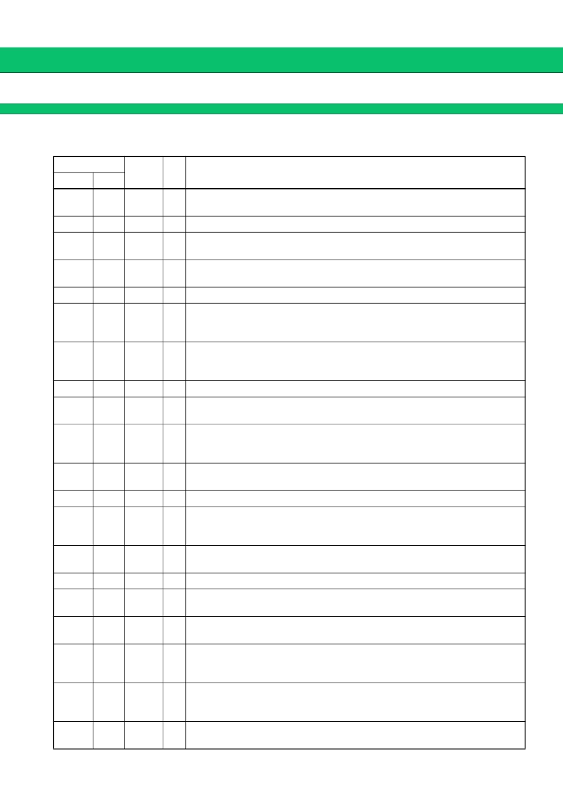
PIN DESCRIPTION
Pin no.
Pin
name
I/O
Descriptions
TSSOP
BCC
1
19
OSC
IN
I
The programmable reference divider input pin. TCXO should be connected with
an AC coupling capacitor.
2
20
GND
Ground pin for OSC input buffer and the shift register circuit.
3
1
fin
IF
I
Prescaler input pin for the IF-PLL.
Connection to an external VCO should be AC coupling.
4
2
Xfin
IF
I
Prescaler complimentary input pin for the IF-PLL section.
This pin should be grounded via a capacitor.
5
3
GND
IF
Ground pin for the IF-PLL section.
6
4
V
CCIF
Power supply voltage input pin for the IF-PLL section (except for the charge
pump circuit) , the shift register and the oscillator input buffer.
When power is OFF, latched data of IF-PLL is lost.
7
5
PS
IF
I
Power saving mode control signal pin for the IF-PLL section. This pin must be set
at “L” when the power supply is started up. (Open is prohibited.)
PS
IF
=
“H”; Normal mode / PS
IF
=
“L”; Power saving mode
Power supply voltage input pin for the IF-PLL charge pump.
8
6
Vp
IF
9
7
Do
IF
O
Charge pump output pin for the IF-PLL section.
Phase characteristics of the phase detector can be reversed by FC-bit.
10
8
LD/fout
O
Look detect signal output (LD) /phase comparator monitoring output (fout) pins.
The output signal is selected by an LDS bit in a serial data.
LDS bit
=
“H”; outputs fout signal / LDS bit
=
“L”; outputs LD signal
Charge pump output pin for the RF-PLL section.
Phase characteristics of the phase detector can be reversed by FC-bit.
11
9
Do
RF
O
12
10
Vp
RF
Power supply voltage input pin for the RF-PLL charge pump.
13
11
PS
RF
I
Power saving mode control pin for the RF-PLL section. This pin must be set at
“L” when the power supply is started up. (Open is prohibited. )
PS
RF
=
“H”; Normal mode / PS
RF
=
“L”; Power saving mode
Power supply voltage input pin for the RF-PLL section (except for the charge
pump circuit) .
14
12
V
CCRF
15
13
GND
RF
Ground pin for the RF-PLL section.
16
14
Xfin
RF
I
Prescaler complimentary input pin for the RF-PLL section.
This pin should be grounded via a capacitor.
17
15
fin
RF
I
Prescaler input pin for the RF-PLL.
Connection to an external VCO should be AC coupling.
18
16
LE
I
Load enable signal input pin (with the schmitt trigger circuit.)
On a rising edge of load enable, data in the shift register is transferred to the cor-
responding latch according to the control bit in a serial data.
19
17
Data
I
Serial data input pin (with the schmitt trigger circuit.)
A data is transferred to the corresponding latch (IF-ref counter, IF-prog. counter,
RF-ref. counter, RF-prog. counter) according to the control bit in a serial data.
20
18
Clock
I
Clock input pin for the 23-bit shift register (with the schmitt trigger circuit.)
One bit data is shifted into the shift register on a rising edge of the clock.
相關(guān)PDF資料 |
PDF描述 |
|---|---|
| MB15F83ULPFT | Fractional-N PLL Frequency Synthesizer |
| MB15F83ULPVA | Fractional-N PLL Frequency Synthesizer |
| MB15F88UL | Fractional-N PLL Frequency Synthesizer |
| MB15F88ULPFT | Fractional-N PLL Frequency Synthesizer |
| MB15F88ULPVA | Fractional-N PLL Frequency Synthesizer |
相關(guān)代理商/技術(shù)參數(shù) |
參數(shù)描述 |
|---|---|
| MB15F83ULPFT | 制造商:FUJITSU 制造商全稱:Fujitsu Component Limited. 功能描述:Fractional-N PLL Frequency Synthesizer |
| MB15F83ULPVA | 制造商:FUJITSU 制造商全稱:Fujitsu Component Limited. 功能描述:Fractional-N PLL Frequency Synthesizer |
| MB15F86UL | 制造商:FUJITSU 制造商全稱:Fujitsu Component Limited. 功能描述:Fractional-N PLL Frequency Synthesizer |
| MB15F86ULPFT | 制造商:FUJITSU 制造商全稱:Fujitsu Component Limited. 功能描述:Fractional-N PLL Frequency Synthesizer |
| MB15F86ULPVA | 制造商:FUJITSU 制造商全稱:Fujitsu Component Limited. 功能描述:Fractional-N PLL Frequency Synthesizer |
發(fā)布緊急采購,3分鐘左右您將得到回復(fù)。