- 您現(xiàn)在的位置:買賣IC網(wǎng) > PDF目錄377880 > MB3841 (Fujitsu Limited) Power Management Switch IC PDF資料下載
參數(shù)資料
| 型號(hào): | MB3841 |
| 廠商: | Fujitsu Limited |
| 英文描述: | Power Management Switch IC |
| 中文描述: | 電源管理開關(guān)IC |
| 文件頁數(shù): | 5/17頁 |
| 文件大小: | 122K |
| 代理商: | MB3841 |
5
MB3841
I
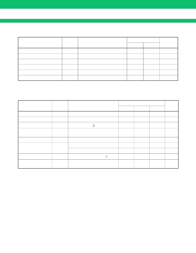
ABSOLUTE MAXIMUM RATINGS
WARNING: Semiconductor devices can be permanently damaged by application of stress (voltage, current,
temperature, etc.) in excess of absolute maximum ratings. Do not exceed these ratings.
I
RECOMMENDED OPERATING CONDITIONS
Note: For C
SS
, R
LIN
settings, see p. 9.
WARNING: The recommended operating conditions are required in order to ensure the normal operation of the
semiconductor device. All of the device's electrical characteristics are warranted when the device is
operated within these ranges.
Always use semiconductor devices within their recommended operating condition ranges. Operation
outside these ranges may adversely affect reliability and could result in device failure.
No warranty is made with respect to uses, operating conditions, or combinations not represented on
the data sheet. Users considering application outside the listed conditions are advised to contact their
FUJITSU representatives beforehand.
Parameter
Symbol
Condition
Rating
Unit
Max.
Min.
Input voltage
V
IN
—
–0.3
7.0
V
Power supply voltage
V
CC
—
–0.3
7.0
V
Control voltage
V
CTL
—
–0.3
7.0
V
Switch current
I
SW
V
IN
= 2.2 V to 5.5 V, Ta = +25
°
C
Ta = +85
°
C
—
—
3 A (DC)
A
Allowable dissipation
P
D
—
280
mW
°
C
Storage temperature
T
STG
–55
+125
Parameter
Symbol
Condition
Value
Unit
Min.
Typ.
Max.
Input voltage
V
IN
—
0
—
5.5
V
Power supply voltage
V
CC
—
0
—
5.5
V
Control voltage
V
CTL
V
CTL
V
CC
0
—
5.5
V
Switch current
I
SW
V
IN
= 2.2 V to 5.5 V,
V
CTL
= 2.2 V to 5.5 V
—
—
2.0
A
SS pin capacitance
C
SS
—
—
—
10
nF
k
k
Current limit
resistance
R
LIN
V
IN
= 5.0 V (I
SW
= 2 A to 0.1 A)
1.8
—
24
V
IN
= 2.2 V (I
SW
= 2 A to 0.1 A)
2.2
—
51
O.C sync current
I
OC
V
IN
= 2.2 V to 5.5 V, V
CC
2.2 V
—
—
1.0
mA
Operating
temperature
T
OP
—
–20
—
+85
°
C
相關(guān)PDF資料 |
PDF描述 |
|---|---|
| MB3841PF-G-BND | PERMASLEEVE WIRE MARKING SLEEVES |
| MB3842 | Power Management 2-ch Switch IC |
| MB3842PFV | Power Management 2-ch Switch IC |
| MB3845 | Power Management 2-ch Switch IC |
| MB3845PFV | Power Management 2-ch Switch IC |
相關(guān)代理商/技術(shù)參數(shù) |
參數(shù)描述 |
|---|---|
| MB3841PF-G-BND | 制造商:FUJITSU 制造商全稱:Fujitsu Component Limited. 功能描述:Power Management Switch IC |
| MB3841PF-G-BND-JNE1 | 制造商:Fujitsu 功能描述:8SOP p[}lWgXCb` Tube |
| MB3842 | 制造商:FUJITSU 制造商全稱:Fujitsu Component Limited. 功能描述:Power Management 2-ch Switch IC |
| MB3842PFV | 制造商:FUJITSU 制造商全稱:Fujitsu Component Limited. 功能描述:Power Management 2-ch Switch IC |
| MB3842PFV-G-BND(E1) | 制造商:Fujitsu 功能描述: |
發(fā)布緊急采購,3分鐘左右您將得到回復(fù)。