- 您現(xiàn)在的位置:買賣IC網(wǎng) > PDF目錄377895 > MB86941 (Fujitsu Limited) Peripheral LSI for SPARClite PDF資料下載
參數(shù)資料
| 型號: | MB86941 |
| 廠商: | Fujitsu Limited |
| 英文描述: | Peripheral LSI for SPARClite |
| 中文描述: | 外圍LSI的SPARClite |
| 文件頁數(shù): | 7/49頁 |
| 文件大小: | 598K |
| 代理商: | MB86941 |
第1頁第2頁第3頁第4頁第5頁第6頁當(dāng)前第7頁第8頁第9頁第10頁第11頁第12頁第13頁第14頁第15頁第16頁第17頁第18頁第19頁第20頁第21頁第22頁第23頁第24頁第25頁第26頁第27頁第28頁第29頁第30頁第31頁第32頁第33頁第34頁第35頁第36頁第37頁第38頁第39頁第40頁第41頁第42頁第43頁第44頁第45頁第46頁第47頁第48頁第49頁
7
MB86941/942
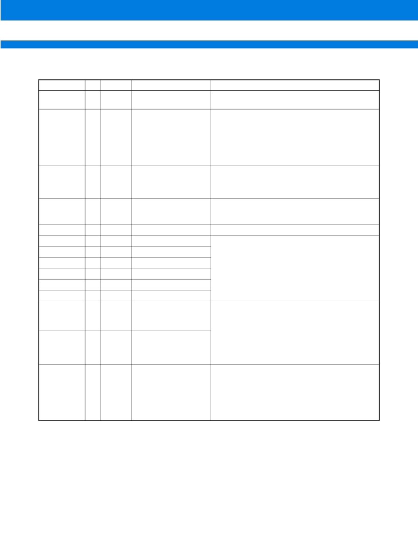
1. MPU INTERFACE SIGNALS (34/33)
(Continued)
Pin symbol
I/O
Pin no.
Pin name
Description
RESET#
I
118
Reset
Reset input pin
Input an “L” signal to this pin to reset the chip.
System clock input pin
The chip contains some modules that use the clock
signal from this pin (not divided), and other modules
that use the clock signal divided in half.
Clock not divided: BIU, RCSTG, IP
Clock divided: IRC, PRS0, PRS1, TM0 to TM3,
SDTR0, SDTR1, SIO
Address strobe input pin
Input an “L” signal to this pin to determine register
access according to the signals input to the RS<5:0>,
CS#, and RD/WR# pins.
Read/write input pin
Input an “H” signal to designate a read cycle, or an “L”
signal to designate a write cycle.
Chip select input pin
CLOCK
I
119
Clock
AS#
I
120
Address Strobe
RD/WR#
I
121
Read/Write
CS#
RS0
RS1
RS2
RS3
RS4
RS5
I
I
I
I
I
I
I
122
135
134
132
131
130
133
Chip Select
Register Select 0
Register Select 1
Register Select 2
Register Select 3
Register Select 4
Register Select 5
Register select input pin
The combination of input signals to the RS<5:0> and
CS# pins determines which register is accessed.
The RS5 pin has internal pull-down resistance
(MB86941 only).
READY1#
O
20
Ready 1
Data ready output pin
MB86941: Open drain output with 12mA “L” drive
capability. Drives an “H” level signal for 3ns
before going to High-Z state.
MB86942: Normal output. READY2# signal deleted. If
the READY generator circuit in the MPU is
used, it is not necessary to connect this pin
to the MPU.
Wait select input pin
Input to this pin determines the interface timing with
the MPU.
Fix “L” to set register read/write access to 3 cycles, or
fix “H” to set register read/write access to 2 cycles.
This pin has internal pull-up resistance (MB86941
only).
READY2#
O
17
Ready 2
WSEL
I
113
Wait Select
相關(guān)PDF資料 |
PDF描述 |
|---|---|
| MB86942 | Peripheral LSI for SPARClite |
| MB86942PFV | Peripheral LSI for SPARClite |
| MB86960 | NETWORK INTERFACE CONTROLLER with ENCODER/DECODER (NICE) |
| MB86960APF-G | NETWORK INTERFACE CONTROLLER with ENCODER/DECODER (NICE) |
| MB86961A | UNIVERSAL INTERFACE FOR 10BASET |
相關(guān)代理商/技術(shù)參數(shù) |
參數(shù)描述 |
|---|---|
| MB86941PFV | 制造商:FUJITSU 制造商全稱:Fujitsu Component Limited. 功能描述:Peripheral LSI for SPARClite |
| MB86942 | 制造商:FUJITSU 制造商全稱:Fujitsu Component Limited. 功能描述:Peripheral LSI for SPARClite |
| MB86942PFV | 制造商:FUJITSU 制造商全稱:Fujitsu Component Limited. 功能描述:Peripheral LSI for SPARClite |
| MB86950BPD-G | 制造商:FUJITSU 功能描述: |
| MB86960 | 制造商:FUJITSU 制造商全稱:Fujitsu Component Limited. 功能描述:NETWORK INTERFACE CONTROLLER with ENCODER/DECODER (NICE) |
發(fā)布緊急采購,3分鐘左右您將得到回復(fù)。