- 您現(xiàn)在的位置:買賣IC網(wǎng) > PDF目錄377895 > MB86960APF-G (Fujitsu Limited) NETWORK INTERFACE CONTROLLER with ENCODER/DECODER (NICE) PDF資料下載
參數(shù)資料
| 型號(hào): | MB86960APF-G |
| 廠商: | Fujitsu Limited |
| 英文描述: | NETWORK INTERFACE CONTROLLER with ENCODER/DECODER (NICE) |
| 中文描述: | 網(wǎng)絡(luò)接口控制器的編碼/解碼器(尼斯) |
| 文件頁(yè)數(shù): | 20/65頁(yè) |
| 文件大小: | 488K |
| 代理商: | MB86960APF-G |
第1頁(yè)第2頁(yè)第3頁(yè)第4頁(yè)第5頁(yè)第6頁(yè)第7頁(yè)第8頁(yè)第9頁(yè)第10頁(yè)第11頁(yè)第12頁(yè)第13頁(yè)第14頁(yè)第15頁(yè)第16頁(yè)第17頁(yè)第18頁(yè)第19頁(yè)當(dāng)前第20頁(yè)第21頁(yè)第22頁(yè)第23頁(yè)第24頁(yè)第25頁(yè)第26頁(yè)第27頁(yè)第28頁(yè)第29頁(yè)第30頁(yè)第31頁(yè)第32頁(yè)第33頁(yè)第34頁(yè)第35頁(yè)第36頁(yè)第37頁(yè)第38頁(yè)第39頁(yè)第40頁(yè)第41頁(yè)第42頁(yè)第43頁(yè)第44頁(yè)第45頁(yè)第46頁(yè)第47頁(yè)第48頁(yè)第49頁(yè)第50頁(yè)第51頁(yè)第52頁(yè)第53頁(yè)第54頁(yè)第55頁(yè)第56頁(yè)第57頁(yè)第58頁(yè)第59頁(yè)第60頁(yè)第61頁(yè)第62頁(yè)第63頁(yè)第64頁(yè)第65頁(yè)
MB86960
receive DMA process before attempting another DMA
process. This is accomplished by writing 00H to
BMPR12. When this is done, the DMA EOP bit will clear
automatically, clearing the EOP status and interrupt, so
it is not necessary to clear the interrupt separately.
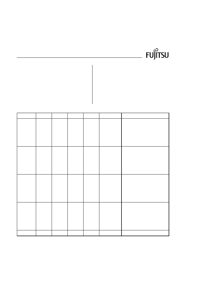
CONTROL AND STATUS REGISTERS
The control and status registers on the NICE chip are
accessed through direct register addresses xxx0H
through xxxFH, and indirect or bank-switching address
bits RBS1, RBS0, DLCR7<3:0>. Table 1 summarizes the
addressing scheme. In system word mode, data can be
transferred 16-bits at a time on the system bus, or 8-bits at
a time by using the byte lane controls of NICE. When
transferring in 16-bit mode to/from the registers, even
direct addresses are used to select the registers. For
example, to access the Transmit/Receive Status Regis-
ters, address xxx0H would be used. The transmit status
would be on the low byte and the receive status on the
high byte. Separate access of high and low bytes is
achieved by using the appropriate byte-access processor
instructions.
Table 1. Internal Register Address Map
RBS1,RBS0
SA3
SA2
SA1
SA0
ADDRESS
DESCRIPTION
XX
XX
XX
XX
XX
XX
XX
XX
0
0
0
0
0
0
0
0
0
0
0
0
1
1
1
1
0
0
1
1
0
0
1
1
0
1
0
1
0
1
0
1
DLCR0
[1]
DLCR1
DLCR2
DLCR3
DLCR4
DLCR5
DLCR6
DLCR7
TRANSMIT STATUS
RECEIVE STATUS
TRANSMIT INT ENABLE
RECEIVE INT ENABLE
TRANSMIT MODE
RECEIVE MODE
CONFIG 0
CONFIG 1
00
00
00
00
00
00
00
00
1
1
1
1
1
1
1
1
0
0
0
0
1
1
1
1
0
0
1
1
0
0
1
1
0
1
0
1
0
1
0
1
DLCR8
DLCR9
DLCR10
DLCR11
DLCR12
DLCR13
DLCR14
DLCR15
NODE ID 0
NODE ID 1
NODE ID 2
NODE ID 3
NODE ID 4
NODE ID 5
TDR 0 (LSB)
TDR 1 (MSB)
01
01
01
01
01
01
01
01
1
1
1
1
1
1
1
1
0
0
0
0
1
1
1
1
0
0
1
1
0
0
1
1
0
1
0
1
0
1
0
1
HT8
HT9
HT10
HT11
HT12
HT13
HT14
HT15
HASH TABLE 0
HASH TABLE 1
HASH TABLE 2
HASH TABLE 3
HASH TABLE 4
HASH TABLE 5
HASH TABLE 6
HASH TABLE 7
10
10
10
10
10
10
10
10
1
1
1
1
1
1
1
1
0
0
0
0
1
1
1
1
0
0
1
1
0
0
1
1
0
1
0
1
0
1
0
1
BMPR8
[2]
BMPR9
BMPR10
BMPR11
BMPR12
BMPR13
BMPR14
BMPR15
BUFFER MEMORY PORT
RESERVED
TRANSMIT START
16 COLLISIONS
DMA ENABLE
DMA BURST
SKIP PACKET
RESERVED
11
X
X
X
X
—
RESERVED
1. All registers are both word and byte accessible. In word mode, register bytes are paired to form words starting with registers 0 and 1. The
odd-addressed byte becomes the high byte of the word
2. In word mode, BMPR8 is a 16-bit port. In byte mode, it is an 8-bit port. The byte ordering Is determined by DLCR7<0>
相關(guān)PDF資料 |
PDF描述 |
|---|---|
| MB86961A | UNIVERSAL INTERFACE FOR 10BASET |
| MB86961APD-G | UNIVERSAL INTERFACE FOR 10BASET |
| MB86961APF-G | UNIVERSAL INTERFACE FOR 10BASET |
| MB86965 | EtherCoupler ETHERNET CONTROLLER WITH 10BASE?T TRANSCEIVER |
| MB86965B | EtherCoupler ETHERNET CONTROLLER WITH 10BASE?T TRANSCEIVER |
相關(guān)代理商/技術(shù)參數(shù) |
參數(shù)描述 |
|---|---|
| MB86961A | 制造商:FUJITSU 制造商全稱:Fujitsu Component Limited. 功能描述:UNIVERSAL INTERFACE FOR 10BASET |
| MB86961APD-G | 制造商:FUJITSU 制造商全稱:Fujitsu Component Limited. 功能描述:UNIVERSAL INTERFACE FOR 10BASET |
| MB86961APF-G | 制造商:FUJITSU 制造商全稱:Fujitsu Component Limited. 功能描述:UNIVERSAL INTERFACE FOR 10BASET |
| MB86965 | 制造商:FUJITSU 制造商全稱:Fujitsu Component Limited. 功能描述:EtherCoupler ETHERNET CONTROLLER WITH 10BASE?T TRANSCEIVER |
| MB86965B | 制造商:FUJITSU 制造商全稱:Fujitsu Component Limited. 功能描述:EtherCoupler ETHERNET CONTROLLER WITH 10BASE?T TRANSCEIVER |
發(fā)布緊急采購(gòu),3分鐘左右您將得到回復(fù)。