- 您現(xiàn)在的位置:買賣IC網(wǎng) > PDF目錄377903 > MB89165A (Fujitsu Limited) 8-Bit Proprietary Microcontroller(8位專用微控制器) PDF資料下載
參數(shù)資料
| 型號: | MB89165A |
| 廠商: | Fujitsu Limited |
| 英文描述: | 8-Bit Proprietary Microcontroller(8位專用微控制器) |
| 中文描述: | 8位微控制器專利(8位專用微控制器) |
| 文件頁數(shù): | 3/59頁 |
| 文件大小: | 508K |
| 代理商: | MB89165A |
第1頁第2頁當(dāng)前第3頁第4頁第5頁第6頁第7頁第8頁第9頁第10頁第11頁第12頁第13頁第14頁第15頁第16頁第17頁第18頁第19頁第20頁第21頁第22頁第23頁第24頁第25頁第26頁第27頁第28頁第29頁第30頁第31頁第32頁第33頁第34頁第35頁第36頁第37頁第38頁第39頁第40頁第41頁第42頁第43頁第44頁第45頁第46頁第47頁第48頁第49頁第50頁第51頁第52頁第53頁第54頁第55頁第56頁第57頁第58頁第59頁
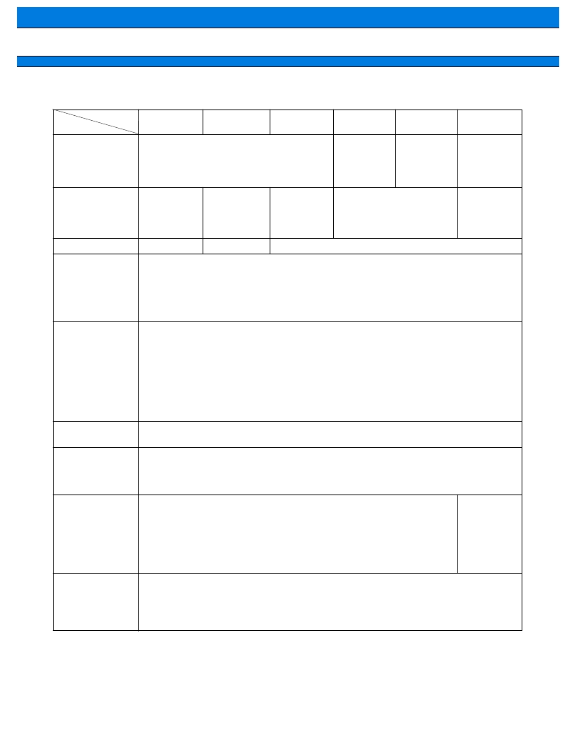
3
MB89160/160A Series
I
PRODUCT LINEUP
(Continued)
MB89161/
MB89161A
*1
MB89163/
MB89163A
*1
MB89165/
MB89165A
*1
MB89P165
MB89W165
MB89PV160
Classification
Mass production products
(mask ROM products)
One-time
PROM
product
EPROM
product
Piggyback/
evaluation
product (for
development)
ROM size
4 K
(internal mask
ROM)
×
8 bits
8 K
(internal mask
ROM)
×
8 bits
16 K
(internal mask
ROM)
×
8 bits
16 K
×
8 bits
(internal PROM programmng with
general-purpose EPROM
programmer)
×
8 bits
136
8 bits
1 to 3 bytes
1, 8,16 bits
0.95
μ
s/4.2 MHz
9
μ
s/4.2 MHz
8 (6 ports also serve as peripherals, 3 ports
are a heavy-current drive type.)
28 (16 ports also serve as segment pins, 2 ports
serve as booster capacitor connection pins,
2 ports serve as common pins.)
(8 ports also serve as an A/D input)
16 (12 ports also serve as an external interrupt)
2 (Also serve as peripherals)
54 (max.)
32 K
(external ROM)
×
8 bits
RAM size
128
×
8 bits
256
×
Number of instructions:
Instruction bit length:
Instruction length:
Data bit length:
Minimum execution time:
Interrupt processing time:
8 bits
512
CPU functions
Ports
I/O port (N-ch open-drain):
Output ports (N-ch open-drain):
*3
I/O ports (CMOS):
Output ports (CMOS):
Total:
Timer/counter
8-bit timer operation (toggled output capable, operating clock cycle 1.9
16-bit timer operation (toggled output capable, operating clock cycle 1.9
μ
μ
s to 486
s to 486
μ
μ
s)
s)
Serial I/O
8 bits
LSB first/MSB first selectability
One clock selectable from four operation clocks
(one external shift clock, three internal shift clocks: 1.9
μ
s, 7.6
μ
s, 30.4
μ
s)
LCD controller/driver
Common output:
Segment output:
Bias power supply pins:
LCD display RAM size:
Booster for LCD driving:
Dividing resistor for LCD driving: Built-in (an external resistor
4 (max.)
24 (max.)
4
24
×
4 bits
Built-in (product with a booster)
*3
*3
selectability)
Without a
booster for
LCD driving
A/D converter
8-bit resolution
×
8 channels
μ
s/4.2 MHz (44 instruction cycles))
μ
s/4.2 MHz)
A/D conversion mode (conversion time 43
Sense mode (conversion time 11.9
Continuous activation by an internal timer capable
Reference voltage input
Part number
Parameter
相關(guān)PDF資料 |
PDF描述 |
|---|---|
| MB89P165 | 8-Bit Proprietary Microcontroller(8位專用微控制器) |
| MB89173L | Hex Inverters 14-CFP -55 to 125 |
| MB89PV170 | 8-bit Proprietary Microcontroller |
| MB89174LPF | 8-bit Proprietary Microcontroller |
| MB89PV170A | 8-bit Proprietary Microcontroller |
相關(guān)代理商/技術(shù)參數(shù) |
參數(shù)描述 |
|---|---|
| MB89165A-PF | 制造商:FUJITSU 制造商全稱:Fujitsu Component Limited. 功能描述:8-bit Proprietary Microcontroller |
| MB89165A-PFS | 制造商:FUJITSU 制造商全稱:Fujitsu Component Limited. 功能描述:8-bit Proprietary Microcontroller |
| MB89165A-PFV | 制造商:FUJITSU 制造商全稱:Fujitsu Component Limited. 功能描述:8-bit Proprietary Microcontroller |
| MB89165-PF | 制造商:FUJITSU 制造商全稱:Fujitsu Component Limited. 功能描述:8-bit Proprietary Microcontroller |
| MB89165-PFS | 制造商:FUJITSU 制造商全稱:Fujitsu Component Limited. 功能描述:8-bit Proprietary Microcontroller |
發(fā)布緊急采購,3分鐘左右您將得到回復(fù)。