- 您現(xiàn)在的位置:買賣IC網(wǎng) > PDF目錄377912 > MB89923PF (FUJITSU LTD) Hex Schmitt-trigger Inverters 14-CDIP -55 to 125 PDF資料下載
參數(shù)資料
| 型號: | MB89923PF |
| 廠商: | FUJITSU LTD |
| 元件分類: | 微控制器/微處理器 |
| 英文描述: | Hex Schmitt-trigger Inverters 14-CDIP -55 to 125 |
| 中文描述: | 8-BIT, MROM, 8 MHz, MICROCONTROLLER, PQFP80 |
| 封裝: | 20 X 14 MM, 0.80 MM PITCH, PLASTIC, QFP-80 |
| 文件頁數(shù): | 3/46頁 |
| 文件大小: | 669K |
| 代理商: | MB89923PF |
第1頁第2頁當前第3頁第4頁第5頁第6頁第7頁第8頁第9頁第10頁第11頁第12頁第13頁第14頁第15頁第16頁第17頁第18頁第19頁第20頁第21頁第22頁第23頁第24頁第25頁第26頁第27頁第28頁第29頁第30頁第31頁第32頁第33頁第34頁第35頁第36頁第37頁第38頁第39頁第40頁第41頁第42頁第43頁第44頁第45頁第46頁
3
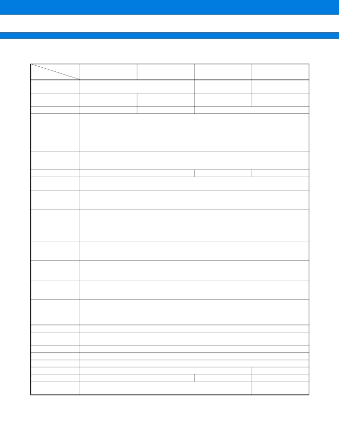
MB89920 Series
I
PRODUCT LINEUP
* :The minimum operating voltage varies with conditions such as the operating frequencies, functions, and
development tool.
MB89925
MB89P928
MB89PV920
Classification
Mass production products
(mask ROM products)
8 K
×
8 bits
(internal mask ROM)
256
×
8 bits
Number of instructions:
Instruction bit length:
Instruction length:
Data bit length:
Minimum execution time:
Interrupt processing time:
I/O ports (CMOS):
I/O ports (N-ch open-drain):
Total:
Specify with mask options
One-time PROM product
(for development)
48 K
×
8 bits
(internal PROM)
Piggyback/evaluation
product (for development)
48 K
×
8 bits
(external ROM)
1024
×
8 bits
ROM size
16 K
×
8 bits
(internal mask ROM)
512
×
8 bits
RAM size
CPU functions
136
8 bits
1 to 3 bytes
1, 8, 16 bits
0.5
μ
s/8 MHz
4.5
μ
s/8 MHz
35 (25 ports also serve as peripherals.)
34 (All also serve as peripherals.)
69
Set with EPROM programmer
Ports
Options
20-bit time-base
timer
Real-time I/O
None
20 bits (interval time selection: 4.10 ms, 16.38 ms, 65.54 ms, 262 ms/8 MHz)
16-bit timer: operating clock cycle (0.5
μ
s, 1.0
μ
s, 2.0
μ
s, 4.0
μ
s), overflow interrupt
Input capture: 16 bits
×
2 channels, external trigger edge selectability
Output compare: 16 bits
×
2 channels
Common output: 4 (selectable from 2 to 4 by software)
Segment output: 28 (can be switched to ports in 4-pin unit by software)
Bias power supply pins: 3
LCD display RAM size: 14
×
8 bits
Dividing resistor for LCD driving: bult-in (external resistor selectability)
8 bits
×
2-channel reload timer operation
8 bits
×
2-channel PWM operation (4 cycles selectable)
8 bits
×
1-channel PPG operation (4 oscillation clocks selectable)
Variable data length (7 or 8 bits), internal baud rate generator, error detection function,
full-duplex with internal double buffer, NRZ transmission formation,
Clock synchronous/asynchronous transfer capable
8 bits, LSB first/MSB first selectability,
One clock selectable from four transfer clocks
(one external shift clock, three internal shift clocks: 1.0
μ
s, 4.0
μ
s, 16.0
μ
s)
10-bit resolution
×
8 channels
A/D conversion mode (conversion time: 16.5
μ
s (33 instruction cycles))
Sense mode (conversion time: 9.0
μ
s (18 instruction cycles))
Continuous activation by an internal clock capable
Interval time: approx. 130 to 260 ms
Reset activation voltage: 3.0 to 4.3 V
Reset release voltage: 3.1 to 4.5 V
Stop the clock oscillation by pin input
1 channel (output a frequency from 1 KHz, 2 KHz, 4 KHz, and divided clock frequency)
4 channels (rising edge/falling edge selectability)
QFP-80
2.2 to 6.0 V*
LCD controller/
driver
8-bit PWM timer
UART
8-bit serial I/O
10-bit A/D
converter
Watchdog timer
Low-voltage
detection reset
Hardware standby
Buzzer/clock output
External interrupt
Package
Operating voltage
EPROM for use
MQFP-80
2.7 to 6.0 V*
MBM27C512-20TV
(LCC package)
2.7 to 6.0 V*
MB89923
Part number
Parameter
相關(guān)PDF資料 |
PDF描述 |
|---|---|
| MB89925 | Hex Schmitt-trigger Inverters 14-CFP -55 to 125 |
| MB89925PF | Hex Schmitt-trigger Inverters 20-LCCC -55 to 125 |
| MB89PV920CF | 8-bit Proprietary Microcontroller |
| MB89930A | 8-bit Proprietary Microcontroller |
| MB8993x | 8-bit Proprietary Microcontroller |
相關(guān)代理商/技術(shù)參數(shù) |
參數(shù)描述 |
|---|---|
| MB89925 | 制造商:FUJITSU 制造商全稱:Fujitsu Component Limited. 功能描述:8-bit Proprietary Microcontroller |
| MB89925PF | 制造商:FUJITSU 制造商全稱:Fujitsu Component Limited. 功能描述:8-bit Proprietary Microcontroller |
| MB8992X | 制造商:FUJITSU 制造商全稱:Fujitsu Component Limited. 功能描述:8-bit Proprietary Microcontroller |
| MB89930A | 制造商:FUJITSU 制造商全稱:Fujitsu Component Limited. 功能描述:8-bit Proprietary Microcontroller |
| MB89935 | 制造商:FUJITSU 制造商全稱:Fujitsu Component Limited. 功能描述:8-bit Proprietary Microcontroller |
發(fā)布緊急采購,3分鐘左右您將得到回復。