- 您現(xiàn)在的位置:買賣IC網(wǎng) > PDF目錄377923 > MB90F345CEPFV (FUJITSU LTD) 16-bit Microcontroller PDF資料下載
參數(shù)資料
| 型號: | MB90F345CEPFV |
| 廠商: | FUJITSU LTD |
| 元件分類: | 微控制器/微處理器 |
| 英文描述: | 16-bit Microcontroller |
| 中文描述: | 16-BIT, FLASH, 24 MHz, MICROCONTROLLER, PQFP100 |
| 封裝: | 14 X 14 MM, 1.70 MM HEIGHT, 0.50 MM PITCH, PLASTIC, LQFP-100 |
| 文件頁數(shù): | 22/84頁 |
| 文件大?。?/td> | 1098K |
| 代理商: | MB90F345CEPFV |
第1頁第2頁第3頁第4頁第5頁第6頁第7頁第8頁第9頁第10頁第11頁第12頁第13頁第14頁第15頁第16頁第17頁第18頁第19頁第20頁第21頁當前第22頁第23頁第24頁第25頁第26頁第27頁第28頁第29頁第30頁第31頁第32頁第33頁第34頁第35頁第36頁第37頁第38頁第39頁第40頁第41頁第42頁第43頁第44頁第45頁第46頁第47頁第48頁第49頁第50頁第51頁第52頁第53頁第54頁第55頁第56頁第57頁第58頁第59頁第60頁第61頁第62頁第63頁第64頁第65頁第66頁第67頁第68頁第69頁第70頁第71頁第72頁第73頁第74頁第75頁第76頁第77頁第78頁第79頁第80頁第81頁第82頁第83頁第84頁
MB90340E Series
22
■
HANDLING DEVICES
1.
Preventing latch-up
CMOS IC may suffer latch
-
up under the following conditions:
A voltage higher than V
CC
or lower than V
SS
is applied to an input or output pin.
A voltage higher than the rated voltage is applied between V
CC
and V
SS
pins.
The AV
CC
power supply is applied before the V
CC
voltage.
Latch-up may increase the power supply current drastically, causing thermal damage to the device.
For the same reason, also be careful not to let the analog power-supply voltage (AV
CC
, AVRH) exceed the digital
power-supply voltage.
Handling unused pins
2.
Leaving unused input terminals open may lead to permanent damage due to malfunction and latch-up; pull up
or pull down the terminals through the resistors of 2 k
or more.
Power supply pins (V
CC
/V
SS
)
If there are multiple V
CC
and V
SS
pins, from the point of view of device design, pins to be of the same potential
are connected inside of the device to prevent malfunction such as latch-up.
To reduce unnecessary radiation, prevent malfunctioning of the strobe signal due to the rise of ground level,
and observe the standard for total output current, be sure to connect the V
CC
and V
SS
pins to the power supply
and ground externally.
Connect V
CC
and V
SS
pins to the device from the current supply source at a possibly low impedance.
As a measure against power supply noise, it is recommended to connect a capacitor of about 0.1
μ
F as a
bypass capacitor between V
CC
and V
SS
pins in the vicinity of V
CC
and V
SS
pins of the device.
3.
4.
Mode Pins (MD0 to MD2)
Connect the mode pins directly to V
CC
or V
SS
pins. To prevent the device unintentionally entering test mode due
to noise, lay out the printed circuit board so as to minimize the distance from the mode pins to V
CC
or V
SS
pins
and to provide a low-impedance connection.
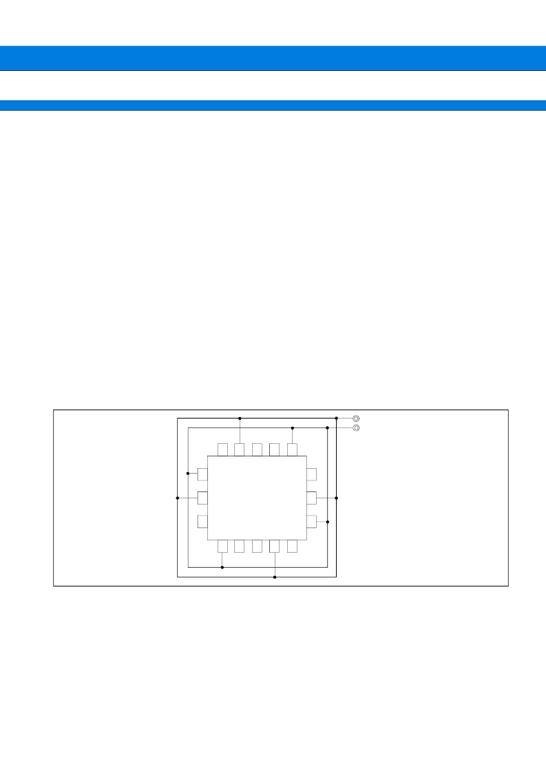
Vcc
Vss
Vss
Vcc
Vss
Vcc
MB90340E
Series
Vcc
Vss
Vcc
Vss
相關PDF資料 |
PDF描述 |
|---|---|
| MB90F345CES | 16-bit Microcontroller |
| MB90F346ES | 16-bit Microcontroller |
| MB90F347ES | 16-bit Microcontroller |
| MB90F349CE | 16-bit Microcontroller |
| MB90F349CES | 16-bit Microcontroller |
相關代理商/技術參數(shù) |
參數(shù)描述 |
|---|---|
| MB90F345CESPMC-GE1 | 制造商:FUJITSU 功能描述: |
| MB90F347ASPMCR-GS-SPE2 | 制造商:FUJITSU 功能描述: |
| MB90F347CAPFR-GSE1 | 制造商:FUJITSU 功能描述: |
| MB90F347CAPFR-GS-SPE1 | 制造商:FUJITSU 功能描述: |
| MB90F347CASPF-GSE1 | 制造商:FUJITSU 功能描述:IC 16BIT MCU CAN 5V SMD QFP100 |
發(fā)布緊急采購,3分鐘左右您將得到回復。