- 您現(xiàn)在的位置:買賣IC網(wǎng) > PDF目錄377923 > MB90F347ES (Fujitsu Limited) 16-bit Microcontroller PDF資料下載
參數(shù)資料
| 型號(hào): | MB90F347ES |
| 廠商: | Fujitsu Limited |
| 英文描述: | 16-bit Microcontroller |
| 中文描述: | 16位微控制器 |
| 文件頁(yè)數(shù): | 15/84頁(yè) |
| 文件大小: | 1098K |
| 代理商: | MB90F347ES |
第1頁(yè)第2頁(yè)第3頁(yè)第4頁(yè)第5頁(yè)第6頁(yè)第7頁(yè)第8頁(yè)第9頁(yè)第10頁(yè)第11頁(yè)第12頁(yè)第13頁(yè)第14頁(yè)當(dāng)前第15頁(yè)第16頁(yè)第17頁(yè)第18頁(yè)第19頁(yè)第20頁(yè)第21頁(yè)第22頁(yè)第23頁(yè)第24頁(yè)第25頁(yè)第26頁(yè)第27頁(yè)第28頁(yè)第29頁(yè)第30頁(yè)第31頁(yè)第32頁(yè)第33頁(yè)第34頁(yè)第35頁(yè)第36頁(yè)第37頁(yè)第38頁(yè)第39頁(yè)第40頁(yè)第41頁(yè)第42頁(yè)第43頁(yè)第44頁(yè)第45頁(yè)第46頁(yè)第47頁(yè)第48頁(yè)第49頁(yè)第50頁(yè)第51頁(yè)第52頁(yè)第53頁(yè)第54頁(yè)第55頁(yè)第56頁(yè)第57頁(yè)第58頁(yè)第59頁(yè)第60頁(yè)第61頁(yè)第62頁(yè)第63頁(yè)第64頁(yè)第65頁(yè)第66頁(yè)第67頁(yè)第68頁(yè)第69頁(yè)第70頁(yè)第71頁(yè)第72頁(yè)第73頁(yè)第74頁(yè)第75頁(yè)第76頁(yè)第77頁(yè)第78頁(yè)第79頁(yè)第80頁(yè)第81頁(yè)第82頁(yè)第83頁(yè)第84頁(yè)
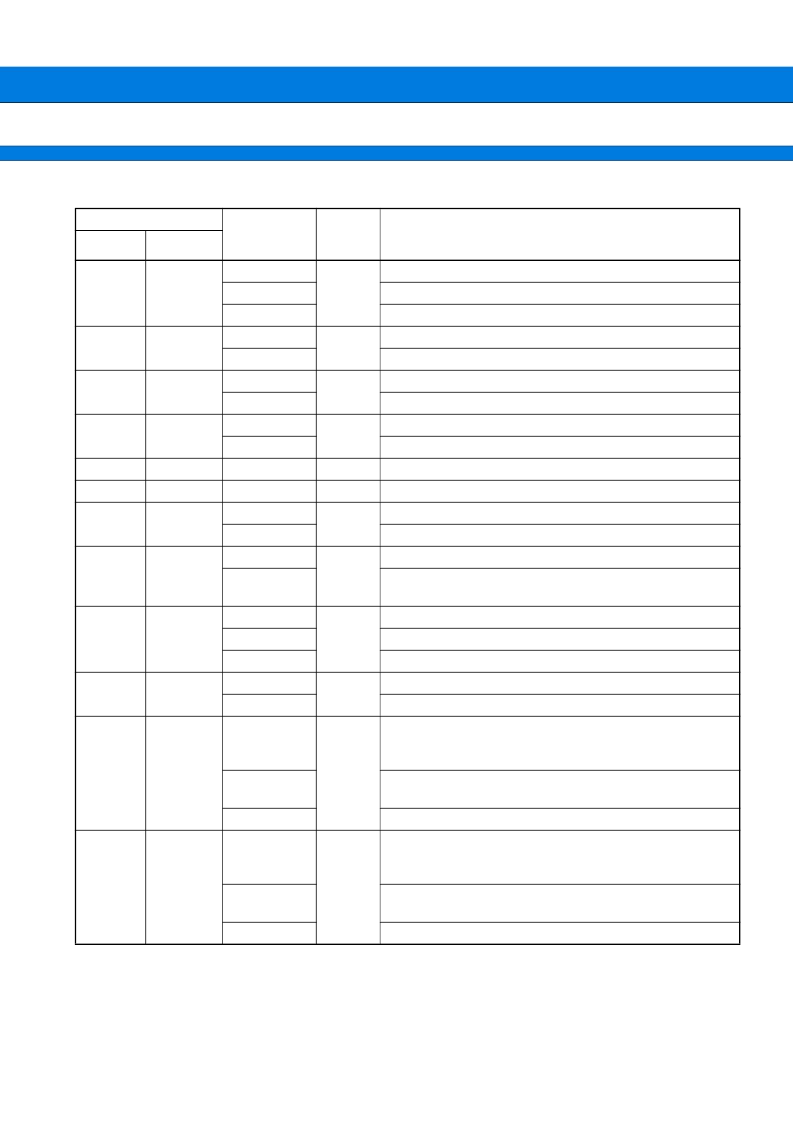
MB90340E Series
15
(Continued)
Pin No.
Pin name
I/O
Circuit
type*
3
Function
QFP100*
1
LQFP100*
2
61
59
P84
SCK0
INT15R
P85
SIN1
P86
SOT1
P87
SCK1
V
CC
V
SS
P90 to P93
PPG1, 3, 5, 7
P94 to P97
OUT0 to
OUT3
PA0
RX0
INT8R
PA1
TX0
F
General purpose I/O pin.
Clock I/O pin for UART0
External interrupt request input pin
General purpose I/O pin.
Serial data input pin for UART1
General purpose I/O pin.
Serial data output pin for UART1
General purpose I/O pin.
Clock I/O pin for UART1
Power (3.5 V to 5.5 V) input pin
GND pin
General purpose I/O pins
Output pins for PPGs
General purpose I/O pins
Waveform output pins for output compares. This function is
enabled when the OCU enables waveform output.
General purpose I/O pin.
RX input pin for CAN0 Interface
External interrupt request input pin
General purpose I/O pin.
TX Output pin for CAN0
General purpose I/O pins. The register can be set to select
whether to use a pull-up resistor. This function is enabled in
single-chip mode.
I/O pins for 8 lower bits of the external address/data bus.
This function is enabled when the external bus is enabled.
External interrupt request input pins.
General purpose I/O pin. The register can be set to select
whether to use a pull-up resistor.
This function is enabled in single-chip mode.
I/O pin for the external address/data bus.
This function is enabled when the external bus is enabled.
Event input pin for the reload timer
62
60
M
63
61
F
64
62
F
65
66
63
64
67 to 70
65 to 68
F
71 to 74
69 to 72
F
75
73
F
76
74
F
77 to 84
75 to 82
P00 to P07
G
AD00 to AD07
INT8 to INT15
85
83
P10
G
AD08
TIN1
相關(guān)PDF資料 |
PDF描述 |
|---|---|
| MB90F349CE | 16-bit Microcontroller |
| MB90F349CES | 16-bit Microcontroller |
| MB90F349E | 16-bit Microcontroller |
| MB90F349ES | 16-bit Microcontroller |
| MB90F342CEPF | 16-bit Microcontroller |
相關(guān)代理商/技術(shù)參數(shù) |
參數(shù)描述 |
|---|---|
| MB90F349ASPFV-GSE1 | 制造商:FUJITSU 功能描述: |
| MB90F349ASPMC-GSE1 | 制造商:FUJITSU 功能描述: |
| MB90F349CAPFR-GSE1 | 制造商:FUJITSU 功能描述: |
| MB90F349CASPFR-GSE1 | 制造商:FUJITSU 功能描述: |
| MB90F349CASPFV-GSE1 | 制造商:FUJITSU 功能描述: |
發(fā)布緊急采購(gòu),3分鐘左右您將得到回復(fù)。