- 您現(xiàn)在的位置:買賣IC網(wǎng) > PDF目錄377918 > MB90F474LPF (FUJITSU LTD) 16-Bit Proprietary Microcontroller PDF資料下載
參數(shù)資料
| 型號(hào): | MB90F474LPF |
| 廠商: | FUJITSU LTD |
| 元件分類: | 微控制器/微處理器 |
| 英文描述: | 16-Bit Proprietary Microcontroller |
| 中文描述: | 16-BIT, FLASH, 12 MHz, MICROCONTROLLER, PQFP100 |
| 封裝: | PLASTIC, QFP-100 |
| 文件頁(yè)數(shù): | 24/118頁(yè) |
| 文件大?。?/td> | 555K |
| 代理商: | MB90F474LPF |
第1頁(yè)第2頁(yè)第3頁(yè)第4頁(yè)第5頁(yè)第6頁(yè)第7頁(yè)第8頁(yè)第9頁(yè)第10頁(yè)第11頁(yè)第12頁(yè)第13頁(yè)第14頁(yè)第15頁(yè)第16頁(yè)第17頁(yè)第18頁(yè)第19頁(yè)第20頁(yè)第21頁(yè)第22頁(yè)第23頁(yè)當(dāng)前第24頁(yè)第25頁(yè)第26頁(yè)第27頁(yè)第28頁(yè)第29頁(yè)第30頁(yè)第31頁(yè)第32頁(yè)第33頁(yè)第34頁(yè)第35頁(yè)第36頁(yè)第37頁(yè)第38頁(yè)第39頁(yè)第40頁(yè)第41頁(yè)第42頁(yè)第43頁(yè)第44頁(yè)第45頁(yè)第46頁(yè)第47頁(yè)第48頁(yè)第49頁(yè)第50頁(yè)第51頁(yè)第52頁(yè)第53頁(yè)第54頁(yè)第55頁(yè)第56頁(yè)第57頁(yè)第58頁(yè)第59頁(yè)第60頁(yè)第61頁(yè)第62頁(yè)第63頁(yè)第64頁(yè)第65頁(yè)第66頁(yè)第67頁(yè)第68頁(yè)第69頁(yè)第70頁(yè)第71頁(yè)第72頁(yè)第73頁(yè)第74頁(yè)第75頁(yè)第76頁(yè)第77頁(yè)第78頁(yè)第79頁(yè)第80頁(yè)第81頁(yè)第82頁(yè)第83頁(yè)第84頁(yè)第85頁(yè)第86頁(yè)第87頁(yè)第88頁(yè)第89頁(yè)第90頁(yè)第91頁(yè)第92頁(yè)第93頁(yè)第94頁(yè)第95頁(yè)第96頁(yè)第97頁(yè)第98頁(yè)第99頁(yè)第100頁(yè)第101頁(yè)第102頁(yè)第103頁(yè)第104頁(yè)第105頁(yè)第106頁(yè)第107頁(yè)第108頁(yè)第109頁(yè)第110頁(yè)第111頁(yè)第112頁(yè)第113頁(yè)第114頁(yè)第115頁(yè)第116頁(yè)第117頁(yè)第118頁(yè)
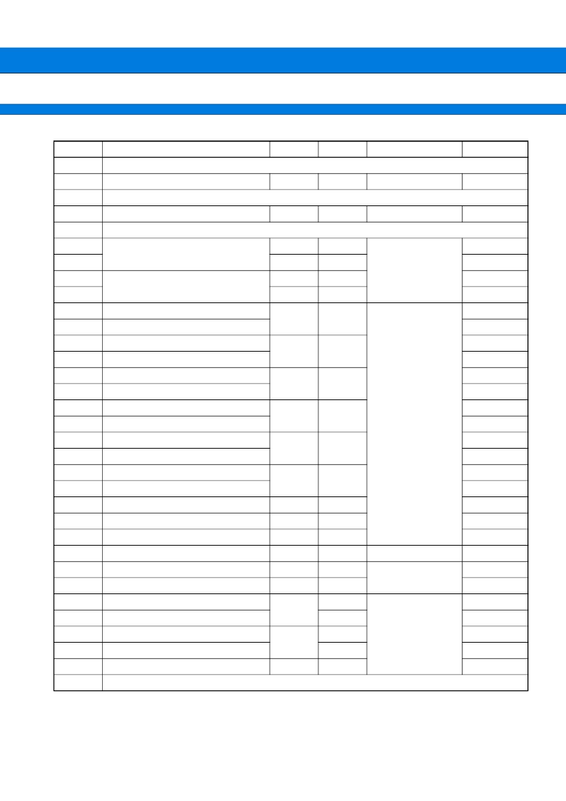
MB90470 Series
24
(Continued)
Address
Register name
Symbol
Access
Resource name
Default
41
H
Reserved
42
H
PPG2, 3 output control register
PPG23
R/W
8/16-bit PPG
0 0 0 0 0 0 0 0
43
H
Reserved
44
H
PPG4, 5 output control register
PPG45
R/W
8/16-bit PPG
0 0 0 0 0 0 0 0
45
H
Reserved
46
H
Control status register
ADCS1
R/W
A/D converter
0 0 0 0 0 0 0 0
47
H
ADCS2
R/W
0 0 0 0 0 0 0 0
48
H
Data register
ADCR1
R
XXXXXXXX
49
H
ADCR2
R
0 0 0 0 0 XXX
4A
H
Output compare register (ch0) low
OCCP0
R/W
16-bit output timer
output compare
(ch0-ch5)
XXXXXXXX
4B
H
Output compare register (ch0) high
XXXXXXXX
4C
H
Output compare register (ch1) low
OCCP1
R/W
XXXXXXXX
4D
H
Output compare register (ch1) high
XXXXXXXX
4E
H
Output compare register (ch2) low
OCCP2
R/W
XXXXXXXX
4F
H
Output compare register (ch2) high
XXXXXXXX
50
H
Output compare register (ch3) low
OCCP3
R/W
XXXXXXXX
51
H
Output compare register (ch3) high
XXXXXXXX
52
H
Output compare register (ch4) low
OCCP4
R/W
XXXXXXXX
53
H
Output compare register (ch4) high
XXXXXXXX
54
H
Output compare register (ch5) low
OCCP5
R/W
XXXXXXXX
55
H
Output compare register (ch5) high
XXXXXXXX
56
H
Output compare control register (ch0)
OCS0
R/W
0 0 0 0 - - 0 0
57
H
Output compare control register (ch1)
OCS1
R/W
- - - 0 0 0 0 0
58
H
Output compare control register (ch2)
OCS2
R/W
0 0 0 0 - - 0 0
59
H
Output compare control register (ch3)
OCS3
R/W
- - - 0 0 0 0 0
5A
H
Output compare control register (ch4)
OCS4
R/W
16-bit output timer
OCU (ch4, 5)
0 0 0 0 - - 0 0
5B
H
Output compare control register (ch5)
OCS5
R/W
- - - 0 0 0 0 0
5C
H
Input capture register (ch0) low
IPCP0
R
16-bit output timer
Input capture (ch0, 1)
XXXXXXXX
5D
H
Input capture register (ch0) high
R
XXXXXXXX
5E
H
Input capture register (ch1) low
IPCP1
R
XXXXXXXX
5F
H
Input capture register (ch1) high
R
XXXXXXXX
60
H
Input capture control register
ICS01
R/W
0 0 0 0 0 0 0 0
61
H
Reserved
相關(guān)PDF資料 |
PDF描述 |
|---|---|
| MB90F474LPFV | 16-Bit Proprietary Microcontroller |
| MB90487PFV | 16-bit Proprietary Microcontroller CMOS |
| MB90F480 | 16-bit Proprietary Microcontroller CMOS |
| MB90F485 | 16-bit Proprietary Microcontroller CMOS |
| MB90F488 | 16-bit Proprietary Microcontroller CMOS |
相關(guān)代理商/技術(shù)參數(shù) |
參數(shù)描述 |
|---|---|
| MB90F474LPFR-GE1 | 制造商:FUJITSU 功能描述: |
| MB90F474LPMCR-GE1 | 制造商:FUJITSU 功能描述: |
| MB90F482PFR-GE1 | 制造商:FUJITSU 功能描述: |
| MB90F482PFR-G-JNE1 | 制造商:FUJITSU 功能描述: |
| MB90F482PMC-G-JNE1 | 制造商:FUJITSU 功能描述: |
發(fā)布緊急采購(gòu),3分鐘左右您將得到回復(fù)。