- 您現(xiàn)在的位置:買賣IC網(wǎng) > PDF目錄377930 > MB90F883SPF (FUJITSU LTD) 16-Bit Proprietary Microcontroller PDF資料下載
參數(shù)資料
| 型號(hào): | MB90F883SPF |
| 廠商: | FUJITSU LTD |
| 元件分類: | 微控制器/微處理器 |
| 英文描述: | 16-Bit Proprietary Microcontroller |
| 中文描述: | 16-BIT, FLASH, 33 MHz, MICROCONTROLLER, PQFP100 |
| 封裝: | 14 X 20 MM, 3.35 MM HEIGHT, 0.65 MM PITCH, PLASTIC, QFP-100 |
| 文件頁數(shù): | 20/75頁 |
| 文件大?。?/td> | 1083K |
| 代理商: | MB90F883SPF |
第1頁第2頁第3頁第4頁第5頁第6頁第7頁第8頁第9頁第10頁第11頁第12頁第13頁第14頁第15頁第16頁第17頁第18頁第19頁當(dāng)前第20頁第21頁第22頁第23頁第24頁第25頁第26頁第27頁第28頁第29頁第30頁第31頁第32頁第33頁第34頁第35頁第36頁第37頁第38頁第39頁第40頁第41頁第42頁第43頁第44頁第45頁第46頁第47頁第48頁第49頁第50頁第51頁第52頁第53頁第54頁第55頁第56頁第57頁第58頁第59頁第60頁第61頁第62頁第63頁第64頁第65頁第66頁第67頁第68頁第69頁第70頁第71頁第72頁第73頁第74頁第75頁
MB90880 Series
20
■
HANDLING DEVICES
1.
Maximum rated voltages for the prevention of latch-up
Be cautious not to exceed the absolute maximum rating.
CMOS ICs may cause latch-up, when a voltage higher than V
CC
or lower than V
SS
is applied to input or output
pins other than medium-to-high resistant pins, or when a voltage exceeding the rating is applied between VCC
and VSS pins.
If latch-up occurs, the power supply current increases rapidly, sometimes resulting in thermal breakdown of the
device. Take the utmost care not to let it occur.
Likewise, care must be taken not to allow the analog power supply (AV
CC
, AVRH) and analog input to exceed
the digital power supply (V
CC
) when turning on or off any analog system.
Handling unused pins
2.
Leaving unused input pins open may cause a malfunction or latch-up which leads to fatal damage to the device.
Therefore, they must be pulled up or down through at least 2 k
resistance. Also, any unused I/O pin should be
left open in the output state, or set to the input state and handled in the same way as an unused input pin.
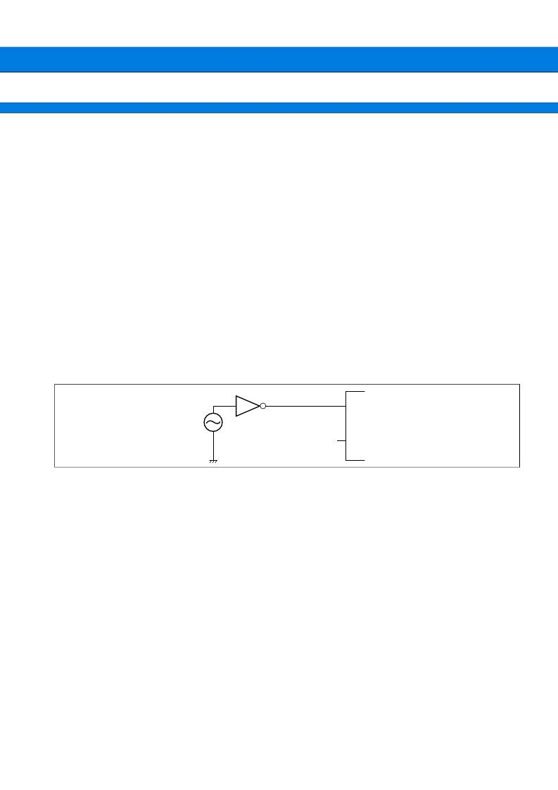
Notes on using external clock
3.
Even when an external clock is being used, oscillation stabilization wait time is required for a power-on reset or
release from sub clock mode or stop mode. Note that 25 MHz is the upper limit on the external clock that can
be used. The following diagram shows an example of using an external clock.
4.
Handling power supply pins (V
CC
/V
SS
)
When multiple VCC and VSS pins supply pins are used, all the power supply pins must be connected to external
power and ground lines due to the device design, to reduce latch-up and unwanted radiation, prevent abnormal
operation of strobe signals caused by the rise in the ground level and to conform to the total output current rating.
Make sure to connect the VCC and VSS pins of this device via lowest impedance to power lines. It is recommended
that a bypass capacitor of around 0.1
μ
F be placed between the VCC and VSS pins near the device.
Crystal oscillator circuit
5.
Noises around X0/X1 or X0A/X1A pins may cause abnormal operations. It is strongly recommended to provide
bypass capacitors via shortest distance from X0/X1, X0A/X1A pins, crystal oscillator (or ceramic oscillator) and
ground lines and also not to allow the lines of the oscillation circuit to cross the lines of other circuits. This will
ensure stable operations of the printed circuit boards. Please ask each crystal maker to evaluate the oscillational
characteristics of the crystal and this device.
6.
Notes on PLL clock mode operation
If an oscillator comes off or clock input stops during PLL clock mode operation, this microcontroller may continue
its operation using a free-running frequency from a self-excited oscillation circuit within PLL. This is not a
guaranteed operation.
X0
X1
Open
相關(guān)PDF資料 |
PDF描述 |
|---|---|
| MB90F883SPMC | 16-Bit Proprietary Microcontroller |
| MB90F884 | 16-Bit Proprietary Microcontroller |
| MB90F884A | 16-Bit Proprietary Microcontroller |
| MB90F884APF | 16-Bit Proprietary Microcontroller |
| MB90F884APMC | 16-Bit Proprietary Microcontroller |
相關(guān)代理商/技術(shù)參數(shù) |
參數(shù)描述 |
|---|---|
| MB90F897PMCR-G-TE1 | 制造商:FUJITSU 功能描述: |
| MB90F897PMT-GSE1 | 制造商:FUJITSU 功能描述:IC 16BIT MCU CAN 5V SMD LQFP48 |
| MB90F897SPMCR-GSE1 | 制造商:FUJITSU 功能描述: 制造商:FUJITSU 功能描述:MCU 16BIT 16LX 64K FLASH 48LQFP 制造商:FUJITSU 功能描述:MCU, 16BIT, 16LX, 64K FLASH, 48LQFP 制造商:FUJITSU 功能描述:IC, 16BIT MCU, F2MC-16LX, 16MHZ, LQFP-48, Controller Family/Series:F2MC-16LX, Core Size:16bit, No. of I/O's:36, Supply Voltage Min:3.5V, Supply Voltage Max:5.5V, Digital IC Case Style:LQFP, No. of Pins:48, Program Memory Size:64KB , RoHS Compliant: Yes 制造商:FUJITSU 功能描述:MCU, 16BIT, 16LX, 64K FLASH, 48LQFP, Controller Family/Series:F2MC-16LX, Core Si |
| MB90F947APFR-GS-SPE1 | 制造商:FUJITSU 功能描述: |
| MB90F962SPMCR-GE1 | 制造商:FUJITSU 功能描述:IC MCU 16BIT 16LX 48LQFP |
發(fā)布緊急采購,3分鐘左右您將得到回復(fù)。