- 您現(xiàn)在的位置:買賣IC網(wǎng) > PDF目錄377930 > MB90P224B (Fujitsu Limited) 8-Bit Proprietary Microcontroller(8位專用微控制器) PDF資料下載
參數(shù)資料
| 型號(hào): | MB90P224B |
| 廠商: | Fujitsu Limited |
| 英文描述: | 8-Bit Proprietary Microcontroller(8位專用微控制器) |
| 中文描述: | 8位微控制器專利(8位專用微控制器) |
| 文件頁數(shù): | 77/105頁 |
| 文件大小: | 1130K |
| 代理商: | MB90P224B |
第1頁第2頁第3頁第4頁第5頁第6頁第7頁第8頁第9頁第10頁第11頁第12頁第13頁第14頁第15頁第16頁第17頁第18頁第19頁第20頁第21頁第22頁第23頁第24頁第25頁第26頁第27頁第28頁第29頁第30頁第31頁第32頁第33頁第34頁第35頁第36頁第37頁第38頁第39頁第40頁第41頁第42頁第43頁第44頁第45頁第46頁第47頁第48頁第49頁第50頁第51頁第52頁第53頁第54頁第55頁第56頁第57頁第58頁第59頁第60頁第61頁第62頁第63頁第64頁第65頁第66頁第67頁第68頁第69頁第70頁第71頁第72頁第73頁第74頁第75頁第76頁當(dāng)前第77頁第78頁第79頁第80頁第81頁第82頁第83頁第84頁第85頁第86頁第87頁第88頁第89頁第90頁第91頁第92頁第93頁第94頁第95頁第96頁第97頁第98頁第99頁第100頁第101頁第102頁第103頁第104頁第105頁
77
MB90220 Series
5. A/D Converter Electrical Characteristics
Single-chip mode MB90223/224/P224B/W224B
: (AV
CC
= V
CC
= +4.5 V to +5.5 V, AV
SS
=V
SS
= 0 V, Ta = –40
°
C to +105
°
C, +4.5 V
≤
AVRH – AVRL
)
MB90P224A/W224A
: (AV
CC
= V
CC
= +4.5 V to +5.5 V, AV
SS
= V
SS
=0 V, Ta = –40
°
C to +85
°
C, +4.5 V
≤
AVRH – AVRL
)
External bus mode
: (AV
CC
= V
CC
= +4.5 V to +5.5 V, AV
SS
= V
SS
=0 V, Ta = –40
°
C to +70
°
C, +4.5 V
≤
AVRH – AVRL)
*1: These standards in this table are for MB90224/P224A/P224B/W224A/W224B.
MB90223: Minimum conversion time is 8.17
μ
s and minimum sampling time is 5
μ
s at t
CYC
= 83.4 ns.
*2: The current value applies to the CPU stop mode with the A/D converter inactive (V
CC
= AV
CC
= AVRH = +5.5 V).
Notes: (1) The error becomes larger as | AVRH – AVRL | becomes smaller.
(2) Use the output impedance of the external circuit for analog input under the following conditions:
External circuit output impedance < approx. 10 k
(Sampling time approx. 3.75
μ
s, t
CYC
= 62.5 ns)
(3) Precision values are standard values applicable to sleep mode.
(4) If V
CC
/AV
CC
or V
SS
/AV
SS
is caused by a noise to drop to below the analog input volgtage, the analog
input current is likely to increase. In such cases, a bypass capacitor or the like should be provided in
the external circuit to suppress the noise.
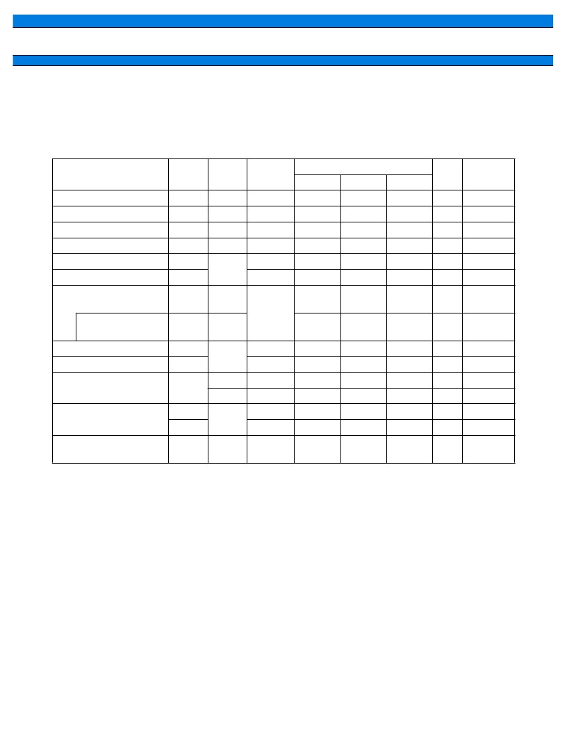
Parameter
Symbol
Pin
name
Condition
Value
Unit
Remarks
Min.
Typ.
Max.
Resolution
n
—
—
—
—
10
±
3.0
±
2.0
±
1.5
bit
Total error
—
—
—
—
—
LSB
Linearity error
—
—
—
—
—
LSB
Differential linearity error
—
—
—
—
—
LSB
Zero transition voltage
V
0T
AN0 to
AN15
—
AVRL – 1.5 AVRL + 0.5 AVRL + 2.5
LSB
Full-scale transition voltage
V
FST
—
AVRH – 3.5 AVRH – 1.5 AVRH + 0.5
LSB
Conversion time*
1
T
CONV
—
t
CYC
= 62.5 ns
6.125
—
—
μ
s
98 machine
cycles
Sampling period
T
SAMP
—
3.75
—
—
μ
s
60 machine
cycles
Analog port input current
I
AIN
AN0 to
AN15
—
—
—
±
0.1
AVRH
μ
A
V
Analog input voltage
V
AIN
—
AVRL
—
Analog reference voltage
—
AVRH
—
AVRL
—
AV
CC
V
AVRL
—
AV
SS
—
AVRH
V
μ
A
μ
A
Reference voltage supply
current
I
R
AVRH
—
—
200
500
I
RH
—
—
—
5*
2
Variation between channels
—
AN0 to
AN15
—
—
—
4
LSB
相關(guān)PDF資料 |
PDF描述 |
|---|---|
| MB90P224BPF | 16-Bit Edge-Triggered D-type Flip-Flops With 3-State Outputs 48-CFP -55 to 125 |
| MB90W224A | 16-bit Proprietary Microcontroller |
| MB90W224B | 16-bit Proprietary Microcontroller |
| MB90W224BZF | 16-bit Proprietary Microcontroller |
| MB90W224ZF | 16-bit Proprietary Microcontroller |
相關(guān)代理商/技術(shù)參數(shù) |
參數(shù)描述 |
|---|---|
| MB90V340A-102CR | 制造商:FUJITSU 功能描述: |
| MB-910 | 制造商:Circuit Test 功能描述:BREADBOARD WIRING KIT - 350 PCS |
| MB9100100 | 制造商:COM/DUO 功能描述:FAN 4-6WKS |
| MB9100-100 | 制造商:COM/DUO 功能描述:FAN 4-6WKS |
| MB91101 | 制造商:Panasonic Industrial Company 功能描述:IC |
發(fā)布緊急采購,3分鐘左右您將得到回復(fù)。