- 您現(xiàn)在的位置:買賣IC網(wǎng) > PDF目錄376149 > MBI5170CD (Electronic Theatre Controls, Inc.) 8-Bit Constant Current LED Sink Driver with Gain Control PDF資料下載
參數(shù)資料
| 型號: | MBI5170CD |
| 廠商: | Electronic Theatre Controls, Inc. |
| 英文描述: | 8-Bit Constant Current LED Sink Driver with Gain Control |
| 中文描述: | 8位恒流增益控制LED驅(qū)動器 |
| 文件頁數(shù): | 3/24頁 |
| 文件大小: | 400K |
| 代理商: | MBI5170CD |

MBI5170 8-Bit Constant Current LED Sink Driver with Gain Control
August 2004, VA.00
- 3 -
T erminal Desc ription
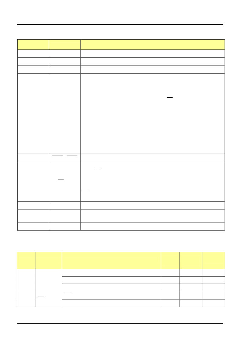
Pin No.
Pin Name
Function
1
GND
Ground terminal for control logic and current sinks
2
SDI
Serial-data input to the Shift Register
3
CLK
Clock input terminal for data shift on rising edge
4
LE/MOD/CA
Output channel data strobe input terminal:
in the Normal Mode phase, serial
data in the Shift Register is transferred to the respective Output Latch when
LE/MOD/CA is high; the data is latched inside the Output Latch when
LE/MOD/CA goes low. If the data in the Output Latch is
“
1
”
(High), the
respective output channel will be enabled after OE /SW is pulled down to low.
Mode selection input terminal:
in the Mode Switching phase, LE/MOD/CA
couldn
’
t strobe serial data but its level is used for determining the next mode to
which MBI5170 is going to switch. When LE/MOD/CA is high, the next mode is
the Current Adjust Mode; when low, the next mode is the Normal Mode.
Configuration data strobe input terminal:
in the Current Adjust Mode phase,
serial data is latched into the Configuration Latch, instead of the Output Latch in
the Normal Mode. The serial data here is regarded as the Configuration Code,
which affect the output current level of all channels.
(See
Operation Principle
)
OUT Constant current output terminals
Output enable terminal:
no matter in what phase MBI5170 operates, the
signal OE /SW can always enable output drivers to sink current. When its level
is (active) low, the output drivers are enabled; when high, all output drivers are
turned OFF (blanked).
Mode switching trigger terminal:
a one-clock-wide short signal pulse of
OE /SW could put MBI5170 into the Mode Switching phase.
(See
Operation Principle
)
SDO
Serial-data output to the following SDI of next driver IC
5-12
OUT0~
7
13
OE /SW
14
15
R-EXT
Input terminal used to connect an external resister for setting up all output
current
16
VDD
Supply voltage terminal
In MBI5170, the relationship between the functions of pin 4 and 13 and the operation phases is listed below:
Pin No.
Pin Name
Function
Normal
Mode
Mode
Switching
Current
Adjust
Mode
No
LE: latching serial data into the Output Latch
Yes
No
MOD: mode selection
No
Yes
No
4
LE/MOD/CA
CA: latching serial data into the Configuration Latch
No
No
Yes
OE: enabling the current output drivers
Yes
Yes
Yes
13
OE/SW
SW: entering the Mode Switching phase
Yes
Yes
Yes
相關(guān)PDF資料 |
PDF描述 |
|---|---|
| MBI5170CDW | 8-Bit Constant Current LED Sink Driver with Gain Control |
| MBI5170CN | 8-Bit Constant Current LED Sink Driver with Gain Control |
| MBI5170CP | 8-Bit Constant Current LED Sink Driver with Gain Control |
| MBR10200CT | 10 Amp HT Power Schottky Barrier Rectifier 100 Volts to 200Volts |
| MBR10200 | 10.0 AMPS. Schottky Barrier Rectifiers |
相關(guān)代理商/技術(shù)參數(shù) |
參數(shù)描述 |
|---|---|
| MBI5170CDW | 制造商:未知廠家 制造商全稱:未知廠家 功能描述:8-Bit Constant Current LED Sink Driver with Gain Control |
| MBI5170CN | 制造商:未知廠家 制造商全稱:未知廠家 功能描述:8-Bit Constant Current LED Sink Driver with Gain Control |
| MBI5170CP | 制造商:未知廠家 制造商全稱:未知廠家 功能描述:8-Bit Constant Current LED Sink Driver with Gain Control |
| MBI5171 | 制造商:未知廠家 制造商全稱:未知廠家 功能描述:8-Bit Constant Current LED Driver with LED Error Detection and Run-Time Current Adjustment |
| MBI5171CD | 制造商:未知廠家 制造商全稱:未知廠家 功能描述:8-Bit Constant Current LED Driver with LED Error Detection and Run-Time Current Adjustment |
發(fā)布緊急采購,3分鐘左右您將得到回復(fù)。