- 您現(xiàn)在的位置:買賣IC網(wǎng) > PDF目錄377936 > MBM29DL164TE70TR (Fujitsu Limited) 16M (2M X 8/1M X 16) BIT Dual Operation PDF資料下載
參數(shù)資料
| 型號(hào): | MBM29DL164TE70TR |
| 廠商: | Fujitsu Limited |
| 英文描述: | 16M (2M X 8/1M X 16) BIT Dual Operation |
| 中文描述: | 16米(2米x 8/1M × 16)位雙操作 |
| 文件頁(yè)數(shù): | 20/75頁(yè) |
| 文件大小: | 1089K |
| 代理商: | MBM29DL164TE70TR |
第1頁(yè)第2頁(yè)第3頁(yè)第4頁(yè)第5頁(yè)第6頁(yè)第7頁(yè)第8頁(yè)第9頁(yè)第10頁(yè)第11頁(yè)第12頁(yè)第13頁(yè)第14頁(yè)第15頁(yè)第16頁(yè)第17頁(yè)第18頁(yè)第19頁(yè)當(dāng)前第20頁(yè)第21頁(yè)第22頁(yè)第23頁(yè)第24頁(yè)第25頁(yè)第26頁(yè)第27頁(yè)第28頁(yè)第29頁(yè)第30頁(yè)第31頁(yè)第32頁(yè)第33頁(yè)第34頁(yè)第35頁(yè)第36頁(yè)第37頁(yè)第38頁(yè)第39頁(yè)第40頁(yè)第41頁(yè)第42頁(yè)第43頁(yè)第44頁(yè)第45頁(yè)第46頁(yè)第47頁(yè)第48頁(yè)第49頁(yè)第50頁(yè)第51頁(yè)第52頁(yè)第53頁(yè)第54頁(yè)第55頁(yè)第56頁(yè)第57頁(yè)第58頁(yè)第59頁(yè)第60頁(yè)第61頁(yè)第62頁(yè)第63頁(yè)第64頁(yè)第65頁(yè)第66頁(yè)第67頁(yè)第68頁(yè)第69頁(yè)第70頁(yè)第71頁(yè)第72頁(yè)第73頁(yè)第74頁(yè)第75頁(yè)
MBM29DL16XTE/BE
-70/90/12
20
I
FUNCTIONAL DESCRIPTION
Simultaneous Operation
MBM29DL16XTE/BE have feature, which is capability of reading data from one bank of memory while a program
or erase operation is in progress in the other bank of memory (simultaneous operation), in addition to the
conventional features (read, program, erase, erase-suspend read, and erase-suspend program). The bank
selection can be selected by bank address (A
15
to A
19
) with zero latency.
The MBM29DL161TE/BE have two banks which contain
Bank 1 (8KB
×
eight sectors) and Bank 2 (64KB
×
thirty-one sectors).
The MBM29DL162TE/BE have two banks which contain
Bank 1 (8KB
×
eight sectors, 64KB
×
three sectors) and Bank 2 (64KB
×
twenty eight sectors).
The MBM29DL163TE/BE have two banks which contain
Bank 1 (8KB
×
eight sectors, 64KB
×
seven sectors) and Bank 2 (64KB
×
twenty four sectors).
The MBM29DL164TE/BE have two banks which contain
Bank 1 (8KB
×
eight sectors, 64KB
×
fifteen sectors) and Bank 2 (64KB
×
sixteen sectors).
The simultaneous operation can not execute multi-function mode in the same bank. Table 10 shows combination
to be possible for simultaneous operation. (Refer to the Figure 11 Bank-to-bank Read/Write Timing Diagram.)
*: An erase operation may also be supended to read from or program to a sector not being erased.
Read Mode
The MBM29DL16XTE/BE have two control functions which must be satisfied in order to obtain data at the outputs.
CE is the power control and should be used for a device selection. OE is the output control and should be used
to gate data to the output pins if a device is selected.
Address access time (t
ACC
) is equal to the delay from stable addresses to valid output data. The chip enable
access time (t
CE
) is the delay from stable addresses and stable CE to valid data at the output pins. The output
enable access time is the delay from the falling edge of OE to valid data at the output pins. (Assuming the
addresses have been stable for at least t
ACC
-t
OE
time.) When reading out a data without changing addresses after
power-up, it is necessary to input hardware reset or to change CE pin from “H” or “L”
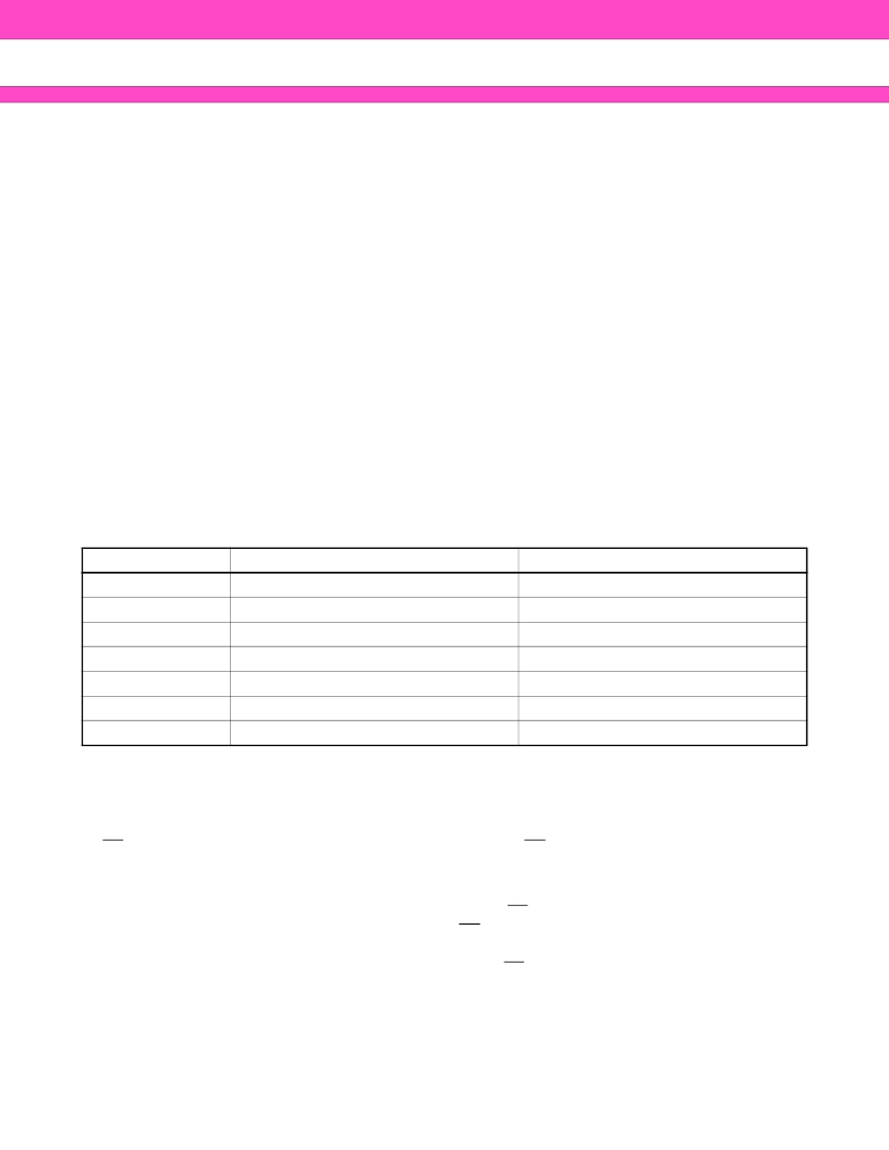
Table 10 Simultaneous Operation
Case
Bank 1 Status
Bank 2 Status
1
Read mode
Read mode
2
Read mode
Autoselect mode
3
Read mode
Program mode
4
Read mode
Erase mode *
5
Autoselect mode
Read mode
6
Program mode
Read mode
7
Erase mode *
Read mode
相關(guān)PDF資料 |
PDF描述 |
|---|---|
| MBM29DL16XTD | 16M (2M x 8/1M x 16) BIT Dual Operation |
| MBM29DL16XTE | 16M (2M X 8/1M X 16) BIT Dual Operation |
| MBM29DL161BE70TN | 16M (2M X 8/1M X 16) BIT Dual Operation |
| MBM29DL161BE70TR | 16M (2M X 8/1M X 16) BIT Dual Operation |
| MBM29DL161TE70PBT | 16M (2M X 8/1M X 16) BIT Dual Operation |
相關(guān)代理商/技術(shù)參數(shù) |
參數(shù)描述 |
|---|---|
| MBM29DL164TE-70TR | 制造商:SPANSION 制造商全稱:SPANSION 功能描述:FLASH MEMORY CMOS 16M (2M X 8/1M X 16) BIT Dual Operation |
| MBM29DL164TE-90 | 制造商:FUJITSU 制造商全稱:Fujitsu Component Limited. 功能描述:16M (2M X 8/1M X 16) BIT Dual Operation |
| MBM29DL164TE-90PBT | 制造商:SPANSION 制造商全稱:SPANSION 功能描述:FLASH MEMORY CMOS 16M (2M X 8/1M X 16) BIT Dual Operation |
| MBM29DL164TE-90TN | 制造商:SPANSION 制造商全稱:SPANSION 功能描述:FLASH MEMORY CMOS 16M (2M X 8/1M X 16) BIT Dual Operation |
| MBM29DL164TE-90TR | 制造商:SPANSION 制造商全稱:SPANSION 功能描述:FLASH MEMORY CMOS 16M (2M X 8/1M X 16) BIT Dual Operation |
發(fā)布緊急采購(gòu),3分鐘左右您將得到回復(fù)。