- 您現(xiàn)在的位置:買賣IC網(wǎng) > PDF目錄377936 > MBM29DL16xBE (Fujitsu Limited) 16M (2MX8/1MX16) BIT Dual Operation PDF資料下載
參數(shù)資料
| 型號: | MBM29DL16xBE |
| 廠商: | Fujitsu Limited |
| 英文描述: | 16M (2MX8/1MX16) BIT Dual Operation |
| 中文描述: | 1,600(2MX8/1MX16)位雙操作 |
| 文件頁數(shù): | 50/75頁 |
| 文件大?。?/td> | 1089K |
| 代理商: | MBM29DL16XBE |
第1頁第2頁第3頁第4頁第5頁第6頁第7頁第8頁第9頁第10頁第11頁第12頁第13頁第14頁第15頁第16頁第17頁第18頁第19頁第20頁第21頁第22頁第23頁第24頁第25頁第26頁第27頁第28頁第29頁第30頁第31頁第32頁第33頁第34頁第35頁第36頁第37頁第38頁第39頁第40頁第41頁第42頁第43頁第44頁第45頁第46頁第47頁第48頁第49頁當(dāng)前第50頁第51頁第52頁第53頁第54頁第55頁第56頁第57頁第58頁第59頁第60頁第61頁第62頁第63頁第64頁第65頁第66頁第67頁第68頁第69頁第70頁第71頁第72頁第73頁第74頁第75頁
MBM29DL16XTE/BE
-70/90/12
50
I
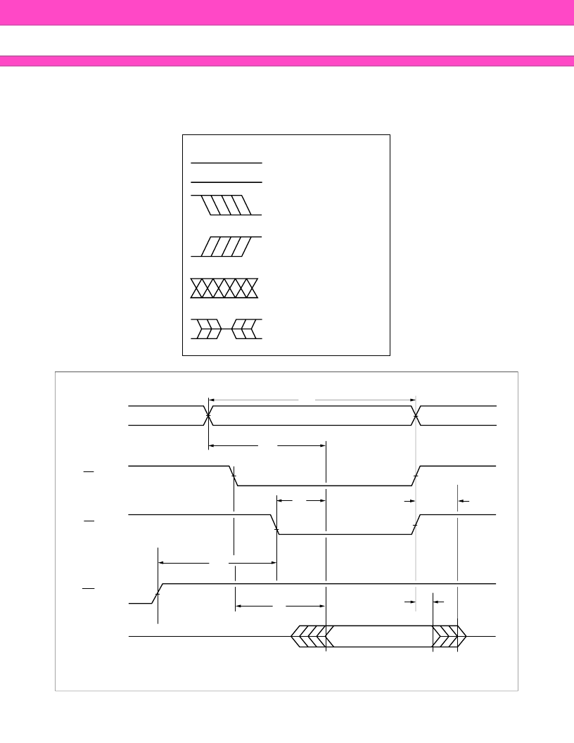
TIMING DIAGRAM
Key to Switching Waveforms
WAVEFORM
INPUTS
OUTPUTS
Must Be
Steady
May
from H to L
May
Change
from L to H
“H” or “L”
Any Change
Permitted
Does Not
Apply
Will Be
Steady
Will Be
Changing
from H to L
Will Be
Changing
from L to H
Changing
State
Unknown
Center Line is
High-
Impedance
“Off” State
WE
OE
CE
t
ACC
t
DF
t
CE
t
OE
Outputs
t
RC
Addresses
Addresses Stable
High-Z
Output Valid
High-Z
t
OEH
t
OH
Figure 5.1 AC Waveforms for Read Operations
發(fā)布緊急采購,3分鐘左右您將得到回復(fù)。