- 您現(xiàn)在的位置:買賣IC網(wǎng) > PDF目錄377939 > MBM29DL322BE-90TN (Fujitsu Limited) 32M (4M x 8/2M x 16) BIT Dual Operation PDF資料下載
參數(shù)資料
| 型號(hào): | MBM29DL322BE-90TN |
| 廠商: | Fujitsu Limited |
| 英文描述: | 32M (4M x 8/2M x 16) BIT Dual Operation |
| 中文描述: | 32M的(4米× 8/2M × 16)位雙操作 |
| 文件頁(yè)數(shù): | 44/80頁(yè) |
| 文件大小: | 1588K |
| 代理商: | MBM29DL322BE-90TN |
第1頁(yè)第2頁(yè)第3頁(yè)第4頁(yè)第5頁(yè)第6頁(yè)第7頁(yè)第8頁(yè)第9頁(yè)第10頁(yè)第11頁(yè)第12頁(yè)第13頁(yè)第14頁(yè)第15頁(yè)第16頁(yè)第17頁(yè)第18頁(yè)第19頁(yè)第20頁(yè)第21頁(yè)第22頁(yè)第23頁(yè)第24頁(yè)第25頁(yè)第26頁(yè)第27頁(yè)第28頁(yè)第29頁(yè)第30頁(yè)第31頁(yè)第32頁(yè)第33頁(yè)第34頁(yè)第35頁(yè)第36頁(yè)第37頁(yè)第38頁(yè)第39頁(yè)第40頁(yè)第41頁(yè)第42頁(yè)第43頁(yè)當(dāng)前第44頁(yè)第45頁(yè)第46頁(yè)第47頁(yè)第48頁(yè)第49頁(yè)第50頁(yè)第51頁(yè)第52頁(yè)第53頁(yè)第54頁(yè)第55頁(yè)第56頁(yè)第57頁(yè)第58頁(yè)第59頁(yè)第60頁(yè)第61頁(yè)第62頁(yè)第63頁(yè)第64頁(yè)第65頁(yè)第66頁(yè)第67頁(yè)第68頁(yè)第69頁(yè)第70頁(yè)第71頁(yè)第72頁(yè)第73頁(yè)第74頁(yè)第75頁(yè)第76頁(yè)第77頁(yè)第78頁(yè)第79頁(yè)第80頁(yè)
MBM29DL32XTE/BE
-80/90/12
44
*: Successive reads from the erasing or erase-suspend sector will cause DQ
2
to toggle. Reading from non-erase
suspend sector address will indicate logic “1” at the DQ
2
bit.
Notes :1.DQ
0
and DQ
1
are reserve pins for future use.
2.DQ
4
is Fujitsu internal use only.
DQ
7
Data Polling
The MBM29DL32XTE/BE devices feature Data Polling as a method to indicate to the host that the Embedded
Algorithms are in progress or completed. During the Embedded Program Algorithm an attempt to read the
devices will produce the complement of the data last written to DQ
7
. Upon completion of the Embedded Program
Algorithm, an attempt to read the device will produce the true data last written to DQ
7
. During the Embedded
Erase Algorithm, an attempt to read the device will produce a “0” at the DQ
7
output. Upon completion of the
Embedded Erase Algorithm an attempt to read the device will produce a “1” at the DQ
7
output. The flowchart
for Data Polling (DQ
7
) is shown in Figure 24.
For programming, the Data Polling is valid after the rising edge of fourth write pulse in the four write pulse
sequence.
For chip erase and sector erase, the Data Polling is valid after the rising edge of the sixth write pulse in the six
write pulse sequence. Data Polling must be performed at sector address within any of the sectors being erased
and not a protected sector. Otherwise, the status may not be valid.
If a program address falls within a protected sector, Data Polling on DQ
7
is active for approximately 1
μ
s, then
that bank returns to the read mode. After an erase command sequence is written, if all sectors selected for
erasing are protected, Data Polling on DQ
7
is active for approximately 400
μ
s, then the bank returns to read mode.
Once the Embedded Algorithm operation is close to being completed, the MBM29DL32XTE/BE data pins (DQ
7
)
may change asynchronously while the output enable (OE) is asserted low. This means that the devices are
driving status information on DQ
7
at one instant of time and then that byte’s valid data at the next instant of time.
Depending on when the system samples the DQ
7
output, it may read the status or valid data. Even if the device
has completed the Embedded Algorithm operation and DQ
7
has a valid data, the data outputs on DQ
0
to DQ
6
may be still invalid. The valid data on DQ
0
to DQ
7
will be read on the successive read attempts.
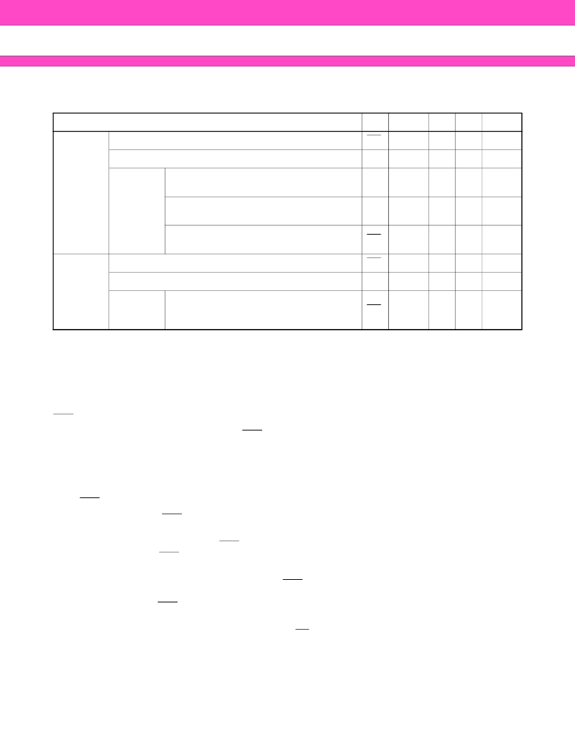
Table 14 Hardware Sequence Flags
Status
DQ
7
DQ
6
DQ
5
DQ
3
DQ
2
In Progress
Embedded Program Algorithm
DQ
7
Toggle
0
0
1
Embedded Erase Algorithm
0
Toggle
0
1
Toggle*
Erase
Suspended
Mode
Erase Suspend Read
(Erase Suspended Sector)
1
1
0
0
Toggle
Erase Suspend Read
(Non-Erase Suspended Sector)
Data
Data
Data Data
Data
Erase Suspend Program
(Non-Erase Suspended Sector)
DQ
7
Toggle
0
0
1*
Exceeded
Time Limits
Embedded Program Algorithm
DQ
7
Toggle
1
0
1
Embedded Erase Algorithm
0
Toggle
1
1
N/A
Erase
Suspended
Mode
Erase Suspend Program
(Non-Erase Suspended Sector)
DQ
7
Toggle
1
0
N/A
相關(guān)PDF資料 |
PDF描述 |
|---|---|
| MBM29DL322BE-90TR | 32M (4M x 8/2M x 16) BIT Dual Operation |
| MBM29DL322BE12PBT | NH FUSE 125A 500V GL/GG SIZE 01 DUAL IN |
| MBM29DL322TD-80 | 32M (4M X 8/2M X 16) BIT Dual Operation |
| MBM29DL322TD-80PBT | 32M (4M X 8/2M X 16) BIT Dual Operation |
| MBM29DL322TD-80PFTN | 32M (4M X 8/2M X 16) BIT Dual Operation |
相關(guān)代理商/技術(shù)參數(shù) |
參數(shù)描述 |
|---|---|
| MBM29DL322BE90TR | 制造商:FUJITSU 制造商全稱:Fujitsu Component Limited. 功能描述:32M (4M x 8/2M x 16) BIT Dual Operation |
| MBM29DL322BE-90TR | 制造商:FUJITSU 制造商全稱:Fujitsu Component Limited. 功能描述:32M (4M x 8/2M x 16) BIT Dual Operation |
| MBM29DL322TD | 制造商:FUJITSU 制造商全稱:Fujitsu Component Limited. 功能描述:32M (4M X 8/2M X 16) BIT Dual Operation |
| MBM29DL322TD-12 | 制造商:FUJITSU 制造商全稱:Fujitsu Component Limited. 功能描述:32M (4M X 8/2M X 16) BIT Dual Operation |
| MBM29DL322TD-80 | 制造商:FUJITSU 制造商全稱:Fujitsu Component Limited. 功能描述:32M (4M X 8/2M X 16) BIT Dual Operation |
發(fā)布緊急采購(gòu),3分鐘左右您將得到回復(fù)。