- 您現(xiàn)在的位置:買賣IC網(wǎng) > PDF目錄377949 > MBM29LV160TE-90 (Fujitsu Limited) 16M (2M X 8/1M X 16) BIT PDF資料下載
參數(shù)資料
| 型號: | MBM29LV160TE-90 |
| 廠商: | Fujitsu Limited |
| 英文描述: | 16M (2M X 8/1M X 16) BIT |
| 中文描述: | 16米(2米x 8/1M × 16)位 |
| 文件頁數(shù): | 22/59頁 |
| 文件大小: | 653K |
| 代理商: | MBM29LV160TE-90 |
第1頁第2頁第3頁第4頁第5頁第6頁第7頁第8頁第9頁第10頁第11頁第12頁第13頁第14頁第15頁第16頁第17頁第18頁第19頁第20頁第21頁當前第22頁第23頁第24頁第25頁第26頁第27頁第28頁第29頁第30頁第31頁第32頁第33頁第34頁第35頁第36頁第37頁第38頁第39頁第40頁第41頁第42頁第43頁第44頁第45頁第46頁第47頁第48頁第49頁第50頁第51頁第52頁第53頁第54頁第55頁第56頁第57頁第58頁第59頁
MBM29LV160TE/BE
-70/90/12
22
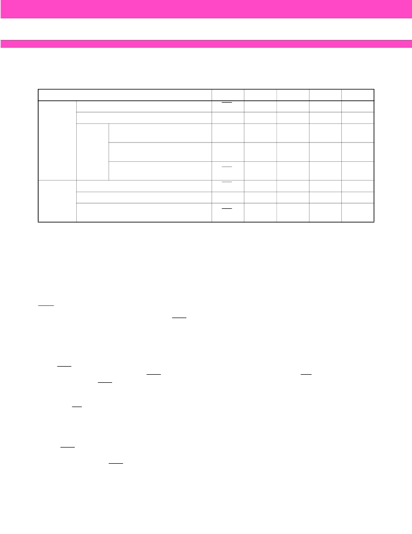
Write Operation Status
Notes: 1. Performing successive read operations from any address will cause DQ
6
to toggle.
2. Reading the byte address being programmed while in the erase-suspend program mode will indicate
logic “1” at the DQ
2
bit. However, successive reads from the erase-suspended sector will cause DQ
2
to
toggle.
3. DQ
0
and DQ
1
are reserve pins for future use.
4. DQ
4
is Fujitsu internal use only.
DQ
7
Data Polling
The MBM29LV160TE/BE device features Data Polling as a method to indicate to the host that the Embedded
Algorithms are in progress or completed. During the Embedded Program Algorithm, an attempt to read the
devices will produce the complement of the data last written to DQ
7
. Upon completion of the Embedded Program
Algorithm, an attempt to read the device will produce the true data last written to DQ
7
. During the Embedded
Erase Algorithm, an attempt to read the device will produce a “0” at the DQ
7
output. Upon completion of the
Embedded Erase Algorithm an attempt to read the device will produce a “1” at the DQ
7
output. The flowchart
for Data Polling (DQ
7
) is shown in Figure 22.
For chip erase and sector erase, Data Polling is valid after the rising edge of the sixth WE pulse in the six-write
pulse sequence. Data Polling must be performed at a sector address within any of the sectors being erased and
not at a protected sector. Otherwise, the status may not be valid. Once the Embedded Algorithm operation is
close to being completed, the MBM29LV160TE/BE data pins (DQ
7
) may change asynchronously while the output
enable (OE) is asserted low. This means that the device is driving status information on DQ
7
at one instant of
time and then that byte’s valid data at the next instant of time. Depending on when the system samples the DQ
7
output, it may read the status or valid data. Even if the device has completed the Embedded Program Algorithm
operation and DQ
7
has a valid data, the data outputs on DQ
0
to DQ
6
may be still invalid. The valid data on DQ
0
to DQ
7
will be read on successive read attempts.
The Data Polling feature is only active during the Embedded Programming Algorithm, Embedded Erase Algorithm
or sector erase time-out.
See Figure 9 for the Data Polling timing specifications and diagram.
Table 8 Hardware Sequence Flags
Status
DQ
7
DQ
7
DQ
6
Toggle
DQ
5
0
DQ
3
0
DQ
2
1
In
Progress
Embedded Program Algorithm
Embedded/Erase Algorithm
0
Toggle
0
1
Toggle
Erase
Suspend
Mode
Erase Suspend Read
(Erase Suspended Sector)
1
1
0
0
Toggle
Erase Suspend Read
(Non-Erase Suspended Sector)
Data
Data
Data
Data
Data
Erase Suspend Program
(Non-Erase Suspended Sector)
DQ
7
Toggle
(Note 1)
0
0
1
(Note 2)
Exceeded
Time
Limits
Embedded Program Algorithm
DQ
7
Toggle
1
0
1
Embedded/Erase Algorithm
0
Toggle
1
1
N/A
Erase Suspend Program
(Non-Erase Suspended Sector)
DQ
7
Toggle
1
0
N/A
相關PDF資料 |
PDF描述 |
|---|---|
| MBM29LV160TE12TN | 16M (2M X 8/1M X 16) BIT |
| MBM29LV160TE12TR | 16M (2M X 8/1M X 16) BIT |
| MBM29LV160TE70PBT | 16M (2M X 8/1M X 16) BIT |
| MBM29LV160TE70TN | 16M (2M X 8/1M X 16) BIT |
| MBM29LV160TE70TR | 16M (2M X 8/1M X 16) BIT |
相關代理商/技術參數(shù) |
參數(shù)描述 |
|---|---|
| MBM29LV160TE90PBT | 制造商:FUJITSU 制造商全稱:Fujitsu Component Limited. 功能描述:16M (2M X 8/1M X 16) BIT |
| MBM29LV160TE90PCV | 制造商:FUJITSU 制造商全稱:Fujitsu Component Limited. 功能描述:16M (2M X 8/1M X 16) BIT |
| MBM29LV160TE90TN | 制造商:Fujitsu 功能描述:Bulk |
| MBM29LV160TE90TR | 制造商:FUJITSU 制造商全稱:Fujitsu Component Limited. 功能描述:16M (2M X 8/1M X 16) BIT |
| MBM29LV160TM90 | 制造商:SPANSION 制造商全稱:SPANSION 功能描述:FLASH MEMORY CMOS 16 M (2M X 8/1M X 16) BIT MirrorFlashTM |
發(fā)布緊急采購,3分鐘左右您將得到回復。