- 您現(xiàn)在的位置:買賣IC網(wǎng) > PDF目錄385562 > MC100EP16VA (ON SEMICONDUCTOR) 3.3V / 5V ECL Differential Receiver/Driver with High Gain(3.3V / 5V ECL差分收發(fā)器(帶高增益)) PDF資料下載
參數(shù)資料
| 型號: | MC100EP16VA |
| 廠商: | ON SEMICONDUCTOR |
| 英文描述: | 3.3V / 5V ECL Differential Receiver/Driver with High Gain(3.3V / 5V ECL差分收發(fā)器(帶高增益)) |
| 中文描述: | 3.3 / 5V的ECL差分接收器/高增益電壓(3.3V / 5V的ECL差分收發(fā)器(帶高增益)驅(qū)動程序) |
| 文件頁數(shù): | 3/8頁 |
| 文件大小: | 76K |
| 代理商: | MC100EP16VA |
MC10EP16VA, MC100EP16VA
http://onsemi.com
3
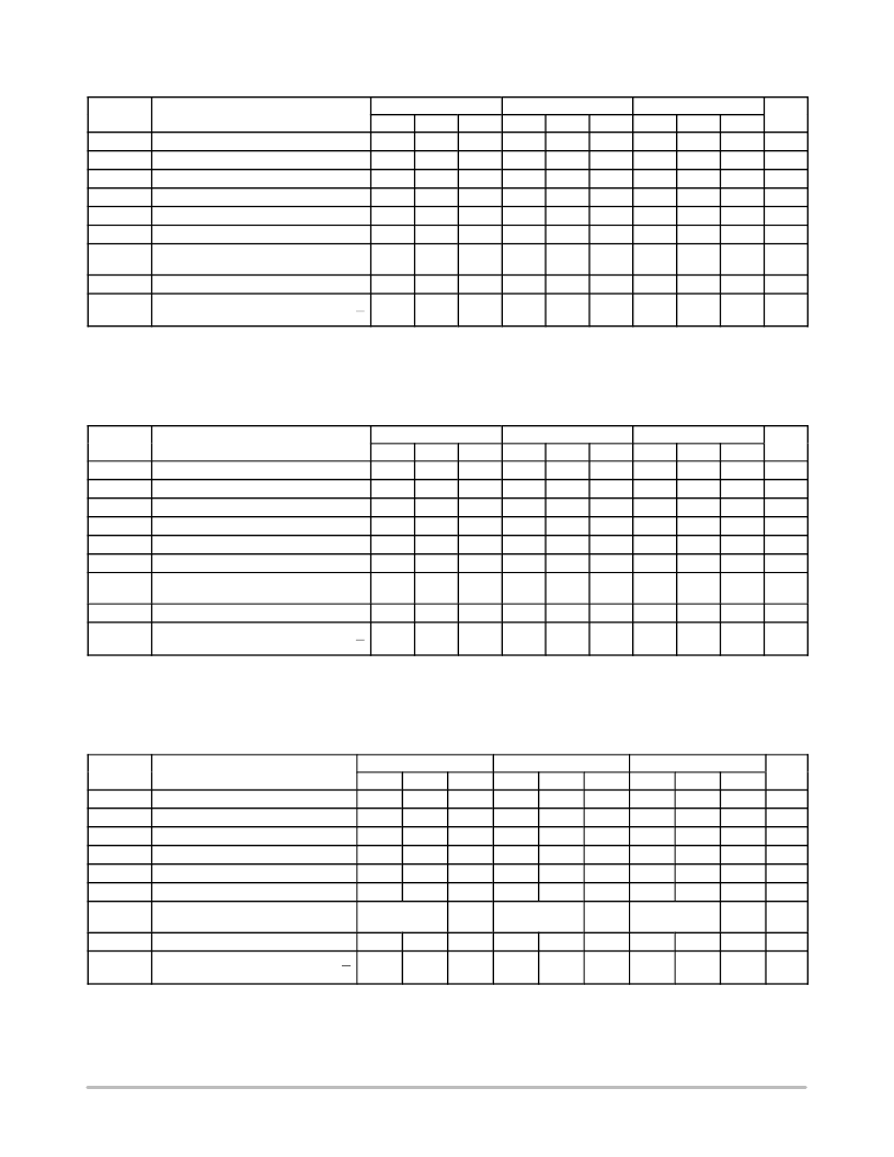
10EP DC CHARACTERISTICS, PECL
V
CC
= 3.3 V, V
EE
= 0 V (Note 2.)
–40
°
C
Typ
24
2290
1490
25
°
C
Typ
24
2355
1555
85
°
C
Typ
24
2415
1615
Symbol
I
EE
V
OH
V
OL
V
IH
V
IL
V
BB
V
IHCMR
Characteristic
Min
20
2165
1365
2090
1365
1790
2.0
Max
31
2415
1615
2415
1690
1990
3.3
Min
20
2230
1430
2155
1460
1855
2.0
Max
31
2480
1680
2480
1755
2055
3.3
Min
20
2290
1490
2215
1490
1915
2.0
Max
32
2540
1740
2540
1815
2115
3.3
Unit
mA
mV
mV
mV
mV
mV
V
Power Supply Current
Output HIGH Voltage (Note 3.)
Output LOW Voltage (Note 3.)
Input HIGH Voltage (Single Ended)
Input LOW Voltage (Single Ended)
Output Voltage Reference
Input HIGH Voltage Common Mode
Range (Differential) (Note 4.)
1890
1955
2015
I
IH
I
IL
Input HIGH Current
Input LOW Current
150
150
150
μ
A
μ
A
D
D
0.5
–150
0.5
–150
0.5
–150
NOTE: EP circuits are designed to meet the DC specifications shown in the above table after thermal equilibrium has been established. The
circuit is in a test socket or mounted on a printed circuit board and transverse airflow greater than 500lfpm is maintained.
2. Input and output parameters vary 1:1 with V
CC
. V
EE
can vary +0.3 V to –2.2 V.
3. All loading with 50 ohms to V
CC
–2.0 volts.
4. V
min varies 1:1 with V
EE
, V
IHCMR
max varies 1:1 with V
CC
. The V
IHCMR
range is referenced to the most positive side of the differential
input signal.
10EP DC CHARACTERISTICS, PECL
V
CC
= 5.0 V, V
EE
= 0 V (Note 5.)
–40
°
C
Symbol
Characteristic
Min
Typ
I
EE
Power Supply Current
20
24
V
OH
Output HIGH Voltage (Note 6.)
3865
3990
V
OL
Output LOW Voltage (Note 6.)
3065
3190
V
IH
Input HIGH Voltage (Single Ended)
3790
V
IL
Input LOW Voltage (Single Ended)
3065
V
BB
Output Voltage Reference
3490
3590
V
IHCMR
Input HIGH Voltage Common Mode
Range (Differential) (Note 7.)
25
°
C
Typ
24
4055
3255
85
°
C
Typ
24
4115
3315
Max
31
4115
3315
4115
3390
3690
5.0
Min
20
3930
3130
3855
3130
3555
2.0
Max
31
4180
3380
4180
3455
3755
5.0
Min
20
3990
3190
3915
3190
3615
2.0
Max
32
4240
3440
4240
3515
3815
5.0
Unit
mA
mV
mV
mV
mV
mV
V
3655
3715
2.0
I
IH
I
IL
Input HIGH Current
Input LOW Current
150
150
150
μ
A
μ
A
D
D
0.5
–150
0.5
–150
0.5
–150
NOTE: EP circuits are designed to meet the DC specifications shown in the above table after thermal equilibrium has been established. The
circuit is in a test socket or mounted on a printed circuit board and transverse airflow greater than 500lfpm is maintained.
5. Input and output parameters vary 1:1 with V
CC
. V
EE
can vary +2.0 V to –0.5 V.
6. All loading with 50 ohms to V
CC
–2.0 volts.
7. V
min varies 1:1 with V
EE
, V
IHCMR
max varies 1:1 with V
CC
. The V
IHCMR
range is referenced to the most positive side of the differential
input signal.
10EP DC CHARACTERISTICS, NECL
V
CC
= 0 V; V
EE
= –5.5 V to –3.0 V (Note 8.)
–40
°
C
Symbol
Characteristic
Min
Typ
I
EE
Power Supply Current
20
24
V
OH
Output HIGH Voltage (Note 9.)
–1135
–1010
V
OL
Output LOW Voltage (Note 9.)
–1935
–1810
V
IH
Input HIGH Voltage (Single Ended)
–1210
V
IL
Input LOW Voltage (Single Ended)
–1935
V
BB
Output Voltage Reference
–1510
–1410
V
IHCMR
Input HIGH Voltage Common Mode
Range (Differential) (Note 10.)
25
°
C
Typ
24
–945
–1745
85
°
C
Typ
24
–885
–1685
Max
31
–885
–1685
–885
–1610
–1310
0.0
Min
20
–1070
–1870
–1145
–1870
–1445
Max
31
–820
–1620
–820
–1545
–1245
0.0
Min
20
–1010
–1810
–1085
–1810
–1385
Max
32
–760
–1560
–760
–1485
–1185
0.0
Unit
mA
mV
mV
mV
mV
mV
V
–1345
–1285
V
EE
+2.0
V
EE
+2.0
V
EE
+2.0
I
IH
I
IL
Input HIGH Current
Input LOW Current
150
150
150
μ
A
μ
A
D
D
0.5
–150
0.5
–150
0.5
–150
NOTE: EP circuits are designed to meet the DC specifications shown in the above table after thermal equilibrium has been established. The
circuit is in a test socket or mounted on a printed circuit board and transverse airflow greater than 500lfpm is maintained.
8. Input and output parameters vary 1:1 with V
CC
.
9. All loading with 50 ohms to V
CC
–2.0 volts.
10.V
min varies 1:1 with V
EE
, V
IHCMR
max varies 1:1 with V
CC
. The V
IHCMR
range is referenced to the most positive side of the differential
input signal.
相關PDF資料 |
PDF描述 |
|---|---|
| MC10EP16VA | 3.3V / 5V ECL Differential Receiver/Driver with High Gain(3.3V / 5V ECL差分收發(fā)器(帶高增益)) |
| MC100EP16VB | 3.3V / 5V ECL Differential Receiver/Driver with High and Low Gain(3.3V / 5V ECL差分收發(fā)器(帶高/低增益)) |
| MC100EP16 | 3.3V / 5V ECL Differential Receiver/Driver(3.3V / 5V ECL差分收發(fā)器) |
| MC100EP57 | 3.3V / 5V ECL 4:1 Differential Multiplexer(3.3V / 5V ECL 4:1差分多路復用器) |
| MC10EP57 | 3.3V / 5V ECL 4:1 Differential Multiplexer(3.3V / 5V ECL 4:1差分多路復用器) |
相關代理商/技術參數(shù) |
參數(shù)描述 |
|---|---|
| MC100EP16VAD | 功能描述:總線收發(fā)器 3.3V/5V ECL Diff RoHS:否 制造商:Fairchild Semiconductor 邏輯類型:CMOS 邏輯系列:74VCX 每芯片的通道數(shù)量:16 輸入電平:CMOS 輸出電平:CMOS 輸出類型:3-State 高電平輸出電流:- 24 mA 低電平輸出電流:24 mA 傳播延遲時間:6.2 ns 電源電壓-最大:2.7 V, 3.6 V 電源電壓-最小:1.65 V, 2.3 V 最大工作溫度:+ 85 C 封裝 / 箱體:TSSOP-48 封裝:Reel |
| MC100EP16VADG | 功能描述:總線收發(fā)器 3.3V/5V ECL Diff RoHS:否 制造商:Fairchild Semiconductor 邏輯類型:CMOS 邏輯系列:74VCX 每芯片的通道數(shù)量:16 輸入電平:CMOS 輸出電平:CMOS 輸出類型:3-State 高電平輸出電流:- 24 mA 低電平輸出電流:24 mA 傳播延遲時間:6.2 ns 電源電壓-最大:2.7 V, 3.6 V 電源電壓-最小:1.65 V, 2.3 V 最大工作溫度:+ 85 C 封裝 / 箱體:TSSOP-48 封裝:Reel |
| MC100EP16VADG | 制造商:ON Semiconductor 功能描述:IC - DRIVER/ RECEIVER |
| MC100EP16VADR2 | 功能描述:總線收發(fā)器 3.3V/5V ECL Diff RoHS:否 制造商:Fairchild Semiconductor 邏輯類型:CMOS 邏輯系列:74VCX 每芯片的通道數(shù)量:16 輸入電平:CMOS 輸出電平:CMOS 輸出類型:3-State 高電平輸出電流:- 24 mA 低電平輸出電流:24 mA 傳播延遲時間:6.2 ns 電源電壓-最大:2.7 V, 3.6 V 電源電壓-最小:1.65 V, 2.3 V 最大工作溫度:+ 85 C 封裝 / 箱體:TSSOP-48 封裝:Reel |
| MC100EP16VADR2G | 功能描述:總線收發(fā)器 3.3V/5V ECL Diff RoHS:否 制造商:Fairchild Semiconductor 邏輯類型:CMOS 邏輯系列:74VCX 每芯片的通道數(shù)量:16 輸入電平:CMOS 輸出電平:CMOS 輸出類型:3-State 高電平輸出電流:- 24 mA 低電平輸出電流:24 mA 傳播延遲時間:6.2 ns 電源電壓-最大:2.7 V, 3.6 V 電源電壓-最小:1.65 V, 2.3 V 最大工作溫度:+ 85 C 封裝 / 箱體:TSSOP-48 封裝:Reel |
發(fā)布緊急采購,3分鐘左右您將得到回復。